Robotic Transfer Technique: The robotic transfer technique enhances scalability of 2D materials for device integration—a phrase that’s shaping the future of electronics and advanced materials. As the demand for smaller, faster, and more energy-efficient devices skyrockets, two-dimensional (2D) materials like graphene and transition metal dichalcogenides (TMDs) are at the heart of this technological leap. However, the challenge of moving these ultra-thin, fragile layers from their growth surfaces to device platforms has long limited their practical use.

Enter robotic automation. This breakthrough is revolutionizing how 2D materials are handled, making it possible to manufacture next-generation devices at industrial scale, with consistent quality and reduced costs. This article will guide you through the science, the process, and the real-world impact of robotic transfer, whether you’re a student, engineer, or business leader.
Table of Contents
Robotic Transfer Technique
| Feature/Fact | Data/Details |
|---|---|
| What are 2D materials? | Atomically thin materials (graphene, TMDs, hBN) with unique electrical, optical, and mechanical properties |
| Main challenge | Manual transfer is slow, inconsistent, and damages materials |
| Robotic transfer throughput | Up to 180 wafers per day |
| Material quality improvement | Fewer defects, higher uniformity, better device performance (graphene mobility >14,000 cm²/V·s) |
| Versatility | Works with graphene, TMDs, hBN, and more |
| Environmental impact | Reduces chemical waste and energy use |
| Professional impact | Enables new device development in electronics, photonics, quantum tech |
| Official resource | bioengineer.org |
The robotic transfer technique marks a turning point for 2D materials, solving the long-standing challenge of moving these fragile, atom-thin layers from lab to device at industrial scale. By combining advanced robotics, interface science, and real-time feedback, this method delivers the speed, quality, and consistency needed for next-generation electronics, photonics, and quantum technologies. As this technology spreads, expect to see 2D materials powering everything from bendable phones to quantum computers—ushering in a new era of innovation.
Understanding 2D Materials: The Building Blocks of Tomorrow

2D materials are substances just one or a few atoms thick. The most famous is graphene—a single layer of carbon atoms arranged in a honeycomb pattern. Others include TMDs (like MoS₂ and WS₂) and hexagonal boron nitride (hBN). These materials are remarkable because they:
- Conduct electricity better than copper
- Are stronger than steel, yet incredibly flexible
- Can be stacked to create new “super materials” (heterostructures)
- Enable ultra-fast, energy-efficient, and even transparent devices
Their unique properties make them ideal for applications in transistors, sensors, flexible electronics, and quantum computing. But their thinness also makes them fragile and difficult to handle.
The Bottleneck: Why Transferring 2D Materials Is So Hard
Traditionally, moving 2D materials from their growth substrate (where they’re made, often using chemical vapor deposition or CVD) to a device surface has been a slow, manual, and error-prone process. The steps often include:
- Coating the 2D material with a support layer (like PMMA)
- Peeling or etching the material off the growth surface
- Placing it onto the target device surface
- Removing the support layer, usually with chemicals
Problems with manual transfer:
- Low throughput: Only a few samples per day
- Inconsistent quality: Tears, wrinkles, and contamination are common
- High cost: Labor-intensive and wasteful
- Environmental concerns: Uses lots of chemicals and energy
These challenges have kept 2D materials from reaching their full potential in commercial devices.
The Breakthrough: Robotic Transfer Technique
How Does Robotic Transfer Work?
The robotic transfer technique uses automated systems—robotic arms, sensors, and machine vision—to move 2D materials with extreme precision. Here’s how it works:
- Automated Preparation: Robots coat the 2D material with a support layer, ensuring even coverage.
- Precision Peeling: Robotic arms gently peel the 2D layer from the growth substrate, using real-time feedback from sensors to avoid rips or wrinkles.
- Target Placement: The robot places the 2D material onto the device surface (silicon, glass, flexible plastic, etc.) with micron-level accuracy.
- Support Removal: The support layer is removed using controlled, low-impact methods (like UV light or gentle solvents), leaving the 2D material clean and intact.
- Quality Assurance: Cameras and sensors inspect each transfer, ensuring only flawless materials are used.
What makes this robotic approach special?
- Industrial-scale throughput: Up to 180 wafers per day—orders of magnitude more than manual methods.
- Uniformity and quality: Consistent, defect-free transfers mean better-performing devices.
- Versatility: Works with a range of 2D materials and supports the creation of complex heterostructures.
- Eco-friendly: Reduces chemical waste and energy use, making it more sustainable.
Technical Innovations: How Robotics Make a Difference
Advanced Interface Science

The robotic system carefully controls the adhesion forces at every step—during pickup, transfer, and deposition. This prevents common problems like tearing, wrinkling, or contamination. By dynamically adjusting these forces, the system keeps the atom-thin sheets pristine, which is essential for high-performance electronics.
Strain Engineering

Even tiny amounts of strain can disrupt the atomic order of 2D materials, ruining their electrical properties. The robotic technique uses precise strain relaxation, ensuring the material stays flat and defect-free. This is especially important for sensitive applications like quantum devices and high-frequency transistors.
Machine Vision and Real-Time Feedback
Robotic arms equipped with cameras and sensors monitor the process in real time. If something goes wrong—like a wrinkle starting to form—the system can adjust instantly. This level of control is impossible with manual methods and is key to achieving industrial consistency.
Practical Applications: Where Robotic Transfer Makes a Difference
Flexible Electronics
Imagine a phone you can fold or a wearable sensor that bends with your body. 2D materials make this possible, but only if they can be transferred cleanly and reliably onto flexible substrates. Robotic transfer makes this a reality by handling even the most delicate materials with care.
Quantum and Photonic Devices

Quantum computers and advanced photonics rely on the perfect stacking of different 2D materials. Any contamination or misalignment can ruin device performance. Robotic transfer enables the precise assembly of these complex structures, opening new frontiers in computing and communications.
Cost and Environmental Benefits
By automating the process, companies save on labor and materials. The system also uses fewer chemicals and less energy, reducing both costs and environmental impact—a win for business and the planet.
Step-by-Step Guide: The Robotic Transfer Process in Detail
- Material Growth: 2D materials are grown using CVD, producing large, high-quality sheets.
- Support Layer Application: A robot applies a thin, even support layer (like PMMA or UV tape).
- Delicate Peeling: Robotic arms, guided by sensors, peel the 2D material off the substrate without damage.
- Precise Placement: The robot places the material onto the target substrate, whether flat, curved, or patterned.
- Support Removal: The support layer is removed using a gentle, controlled method (e.g., UV light, low-temperature solvents).
- Inspection: Machine vision checks for defects, ensuring only perfect materials are used in devices.
- Integration: The 2D material is now ready for further processing—such as patterning, stacking, or device fabrication.
Industry Impact: Why This Matters for Professionals
- Researchers: Can now experiment with large batches of high-quality 2D materials, speeding up innovation and discovery.
- Manufacturers: Gain access to industrial-scale production, making it feasible to include 2D materials in mainstream products.
- Startups: Lower barriers to entry for new companies looking to develop flexible electronics, sensors, or quantum devices.
- Environmental Managers: Benefit from reduced waste and energy use, helping meet sustainability goals.
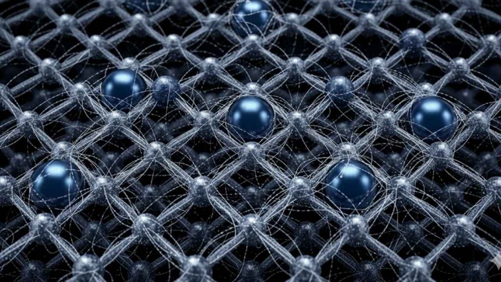
Discovery Of New 2D Material Confirms Decade-Old Prediction, Opening Doors For Advanced Electronics
Child Who Received CAR-T Cancer Therapy Remains Disease-Free 18 Years Later
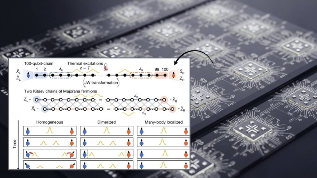
Quantum Computing Milestone Achieved, Immediately Challenged by Supercomputer
FAQs About Robotic Transfer Technique
Q1: What are the main benefits of robotic transfer over manual methods?
A: Robotic transfer is faster (up to 180 wafers/day), more consistent, less damaging to materials, and more environmentally friendly.
Q2: Can robotic transfer handle all types of 2D materials?
A: Yes, it’s versatile—works with graphene, TMDs, hBN, and more. The system can be tuned for different material properties.
Q3: Is the process suitable for mass production?
A: Absolutely. The high throughput and consistent quality make it ideal for industrial-scale manufacturing.
Q4: How does robotic transfer affect device performance?
A: Devices made with robotically transferred 2D materials have higher mobility, fewer defects, and more reliable performance.
Q5: Where can I learn more about the technology?
A: For more information, explore resources on advanced materials and robotic automation in electronics manufacturing.
The Future: What’s Next for Robotic Transfer and 2D Materials?
The robotic transfer technique is already enabling new products and research breakthroughs. As technology advances, expect to see:
More complex heterostructures: Stacking different 2D materials for custom electronic and optical properties.
- Integration with Industry 4.0: Smart factories using AI and robotics for fully automated device manufacturing.
- Expansion to new substrates: Flexible, curved, or even bio-compatible surfaces for medical devices and wearables.
- Further environmental gains: Even greener processing as automation reduces chemical and energy use.