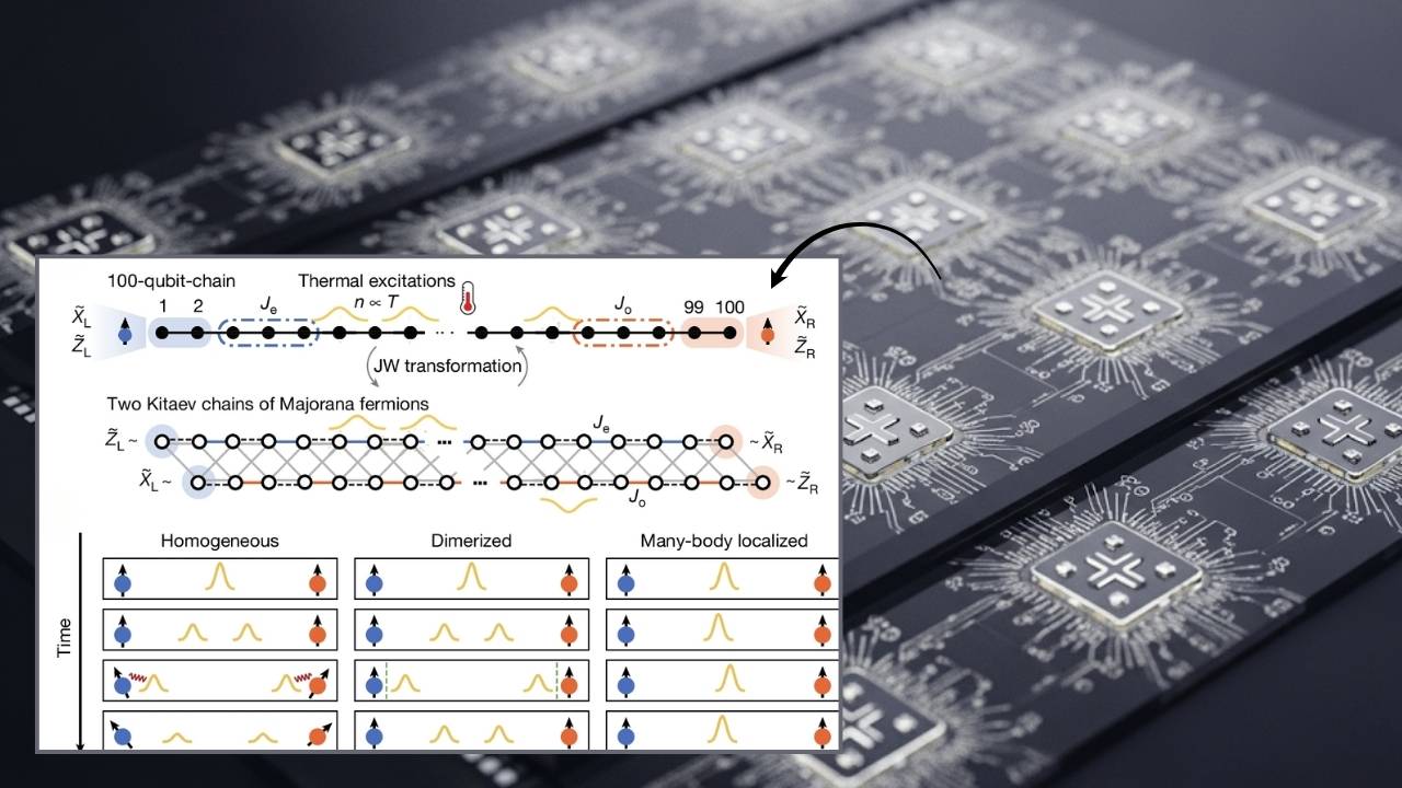
Quantum Sensing Using 2D Materials: Physicists at the University of Cambridge have announced a major breakthrough in quantum sensing using 2D materials for next-generation nanoscale devices. This achievement, published in a leading scientific journal, marks a pivotal moment for quantum technology, opening new frontiers in how we detect, visualize, and manipulate the tiniest physical phenomena.

Leveraging the unique properties of hexagonal boron nitride (hBN), a material just one atom thick, researchers have crafted sensors that far surpass the capabilities of previous technologies, setting the stage for a new era in science and engineering.
Quantum Sensing Using 2D Materials
| Feature/Topic | Details & Stats |
|---|---|
| What are 2D Materials? | Atomically thin materials like graphene and hBN, with unique electronic and optical properties |
| Breakthrough Material | Hexagonal boron nitride (hBN) with engineered spin defects, enabling room-temperature, multi-axis quantum sensing |
| Key Innovation | Multi-axis, high-dynamic-range magnetic field detection at the nanoscale |
| Real-World Applications | Nanoscale imaging, quantum computing, secure communications, advanced electronics |
| Career Pathways | Materials science, quantum engineering, nanotechnology, electronics |
| Official Resource |
The breakthrough in quantum sensing using 2D materials for next-generation nanoscale devices is more than just a scientific achievement—it’s a leap toward a future where we can see, measure, and control the quantum world with unprecedented clarity. With hBN leading the charge, quantum sensors are set to revolutionize everything from electronics and energy to medicine and communications. As research continues, the possibilities for discovery and innovation are virtually limitless.
What Are 2D Materials?

2D materials are substances that are only one or a few atoms thick. The most famous is graphene, but others like hexagonal boron nitride (hBN) and molybdenum disulfide (MoS₂) are equally exciting. Because they are so thin, these materials display properties—such as high surface area, flexibility, and quantum effects—that are not found in their bulk counterparts.
- Atomic Thinness: Imagine a sheet so thin you can’t see it under a regular microscope. That’s what we’re talking about!
- Unique Properties: Electrons move differently, light interacts in new ways, and even heat and sound behave unusually in 2D materials.
What Is Quantum Sensing?
Quantum sensing harnesses the strange laws of quantum physics—like superposition and entanglement—to measure things with extreme sensitivity and precision. These sensors can detect incredibly small changes in magnetic fields, temperature, or pressure—sometimes down to the level of single atoms.

- Spin Defects: Tiny imperfections in a material’s atomic structure that can act as quantum sensors.
- Optical Readout: By shining light on these defects, scientists can “read” their quantum state, which changes in response to their environment.
Why Is hBN a Game-Changer for Quantum Sensing?
From Diamond to hBN: The Evolution of Quantum Sensors
Until now, the gold standard for quantum sensing was the nitrogen-vacancy (NV) center in diamond. These defects allowed for single-axis magnetic field detection at room temperature. However, NV centers have limitations: they can only sense along one direction and have a limited range for detecting magnetic fields.
hBN changes the game:
- Multi-Axis Sensing: hBN-based sensors can detect magnetic fields in multiple directions at once, giving a more complete picture of what’s happening at the nanoscale.
- Room-Temperature Operation: Like diamond, hBN sensors work at room temperature, making them practical for real-world applications.
- Ultra-Thin and Flexible: hBN is just one atom thick, so sensors can be placed extremely close to what they’re measuring, improving spatial resolution.
- Superior Integration: hBN can be easily combined with other 2D materials, creating customizable sensor platforms for various applications.

“This work takes that capability to the next level using hBN, a material that’s not only compatible with nanoscale applications but also offers new degrees of freedom compared to state-of-the-art nanoscale quantum sensors.”
— Dr Carmem Gilardoni, University of Cambridge
How Does Quantum Sensing with hBN Work?
Step-by-Step Guide
Step 1: Creating High-Quality hBN
Researchers grow or exfoliate ultra-thin sheets of hBN using advanced techniques like chemical vapor deposition (CVD) or mechanical peeling. The quality of the material is crucial for effective sensing.
Step 2: Engineering Spin Defects
Defects, such as boron vacancies, are intentionally introduced into the hBN lattice. These act as quantum sensors, with their electron spins sensitive to environmental changes.
Step 3: Optical Excitation and Readout
A laser excites the spin defect. The defect then emits light (photoluminescence), which changes depending on the local magnetic field, temperature, or pressure.
Step 4: Data Analysis
The emitted light is analyzed using sensitive detectors and computers, allowing researchers to map out physical properties at the nanoscale.
Example:
If a sheet of hBN with engineered defects is placed near a tiny wire, the defects will “feel” the magnetic field from the current in the wire. By scanning the sheet, scientists can create a highly detailed map of the current flow—down to the atomic level.
Real-World Applications
1. Nanoscale Imaging and Magnetometry
hBN quantum sensors can visualize magnetic fields and current flows in materials with unprecedented detail. This is crucial for developing next-generation electronics and discovering new physical phenomena.
2. Quantum Computing and Communication
hBN’s single-photon emitters (SPEs) are essential for secure quantum communication and scalable quantum computers. These emitters can generate one photon at a time, a key requirement for quantum cryptography and information processing.
3. Advanced Electronics and Energy
hBN’s resilience and stability make it ideal for protecting microchips, enabling faster transistors, and supporting greener energy solutions such as hydrogen storage and fuel cell catalysts.
4. Sensing in Harsh Environments
Because hBN is chemically stable and can withstand high temperatures, it’s perfect for sensors in extreme conditions—like aerospace, nuclear reactors, or deep-sea exploration.
The Science Behind the Breakthrough
Spin Defects and Quantum States
At the heart of hBN’s sensing power are its spin defects, particularly the negatively charged boron vacancy. These defects can be controlled and read out using light—a process known as optically detected magnetic resonance (ODMR). This allows for atomic-scale detection of magnetic fields, temperature, and even pressure at room temperature.

- Single-Photon Emitters (SPEs): These defects can emit one photon at a time, which is crucial for quantum communication and ultra-sensitive detection.
- Charge State Control: Recent advances have enabled scientists to stabilize and manipulate the charge states of these defects, overcoming a major hurdle that limited earlier applications.
Integration and Customization
hBN’s van der Waals structure means it can be easily stacked with other 2D materials, creating custom sensor arrays and devices tailored for specific tasks. This modularity is a huge advantage over bulkier, less flexible materials.
Challenges and Future Directions
Current Challenges
- Material Quality: Producing large, defect-free sheets of hBN remains a technical challenge.
- Defect Engineering: Precisely controlling the type, location, and charge state of defects is still a developing science.
- Integration: Combining hBN sensors with existing electronic and optical systems at scale is complex.
Opportunities and Next Steps
- Scalable Manufacturing: Advances in material growth and defect engineering will make hBN sensors more widely available.
- New Applications: As understanding grows, expect to see hBN sensors in biomedical imaging, environmental monitoring, and even consumer electronics.
- Interdisciplinary Research: The field brings together physics, chemistry, engineering, and computer science, creating exciting new career opportunities.
Physicists Create One of the Most Neutron-Deficient Isotopes Ever Observed in the Lab
Attosecond ‘Clock’ Measures Electron Tunneling Time With Unmatched Precision
New Polymer Breakthrough Boosts Durability and Sustainability Using Green Chemistry
FAQs About Quantum Sensing Using 2D Materials
What makes hBN better than diamond for quantum sensing?
hBN offers multi-axis sensing, a broader dynamic range, and superior integration with other 2D materials. It also enables atomic-scale proximity to the sample, which is hard to achieve with diamond.
Can hBN sensors work at room temperature?
Yes, hBN-based quantum sensors operate effectively at room temperature, making them practical for real-world use.
What are single-photon emitters and why are they important?
Single-photon emitters produce one photon at a time, essential for secure quantum communication and advanced quantum computing.
How are defects introduced into hBN?
Defects can be engineered during material growth or by using techniques like electron beam irradiation and optical excitation.
Where can I learn more or get involved?
Explore the QUT 2D Materials for Quantum Technologies project for research updates and opportunities.
Practical Advice for Students and Professionals
- Stay Informed: Follow reputable journals and university research groups for the latest developments in quantum sensing and 2D materials.
- Get Hands-On Experience: Seek internships or research assistant roles in labs working on quantum materials or nanotechnology.
- Build a Strong Foundation: Master the basics of quantum mechanics, solid-state physics, and materials science.
- Network and Collaborate: Attend conferences, workshops, and webinars to connect with experts and peers in the field.