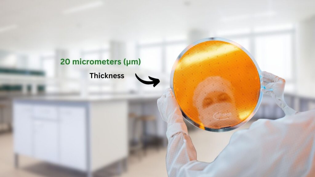
World’s Thinnest Silicon-Based Material: The world’s thinnest silicon-based material has just been unveiled, marking a groundbreaking leap in the field of next-generation 2D electronics. At the heart of this innovation is Infineon Technologies AG, a global leader in semiconductor solutions, which has successfully engineered and mass-produced silicon power wafers just 20 micrometers thick—a feat that redefines what’s possible in both energy efficiency and device performance.
This breakthrough is not just a technical marvel; it’s a practical game-changer for industries ranging from artificial intelligence (AI) and data centers to consumer electronics and motor control. In this article, we’ll explore what makes this ultra-thin silicon material so special, how it’s made, why it matters, and what it means for the future of technology.
World’s Thinnest Silicon-Based Material
| Feature/Fact | Details |
|---|---|
| Material Thickness | 20 micrometers (µm) – a quarter the thickness of a human hair |
| Industry Standard Thickness | 40–60 µm |
| Manufacturer | Infineon Technologies AG |
| Diameter | 300 millimeters (mm) |
| Reduction in Substrate Resistance | 50% less than conventional wafers |
| Reduction in Power Loss | Over 15% improvement |
| Main Applications | AI data centers, computing, motor control, consumer electronics |
| Commercial Availability | Already qualified, released to customers, and showcased at electronica 2024 |
| Official Resource | Infineon Ultra-Thin Silicon Power Wafer Technology |
The unveiling of the world’s thinnest silicon-based material by Infineon Technologies is a landmark achievement for the semiconductor industry and a major step toward a more efficient, sustainable, and powerful digital world. With practical benefits for AI, consumer electronics, and beyond, this innovation is set to shape the next generation of 2D electronics and pave the way for future breakthroughs in materials science.
What Is the World’s Thinnest Silicon-Based Material?
Silicon wafers are the foundation of nearly every electronic device you use—from smartphones to supercomputers. Traditionally, these wafers are sliced to a thickness of 40 to 60 micrometers for power electronics. Infineon’s new 20-micrometer wafer is half as thick as today’s industry standard and just a quarter the thickness of a human hair.
Why does thickness matter? In electronics, thinner wafers mean less resistance for electricity to flow through, which leads to less heat, lower energy loss, and more efficient devices. This is especially important as our world becomes more digital and energy-hungry, with AI and cloud computing driving up the need for powerful, efficient hardware.
How Was This Breakthrough Achieved?
Overcoming Technical Challenges
Making silicon wafers thinner is not as simple as just slicing them down. The process introduces several challenges:
- Wafer Handling: Ultra-thin wafers are fragile and prone to bending or breaking during manufacturing.
- Backside Processing: The metal stack that connects the chip is often thicker than the wafer itself, complicating assembly.
- Wafer Bow and Separation: Thinner wafers can warp or separate, affecting quality and yield.
To solve these issues, Infineon developed innovative wafer grinding and handling techniques, ensuring the wafers remain robust enough for high-volume production and real-world use.
Seamless Integration
One of the most impressive aspects of Infineon’s technology is its ability to integrate seamlessly into existing high-volume silicon production lines. This means manufacturers can adopt the new wafer technology without overhauling their entire process, making the transition to more efficient electronics smoother and faster.
Why Is This Important? Practical Benefits and Real-World Impact
1. Energy Efficiency
By halving the wafer thickness, substrate resistance is reduced by 50%, which translates into over 15% less power loss in systems using these wafers. This is a huge gain for any application where energy efficiency is critical, such as data centers running thousands of servers 24/7.
2. Power Density and Performance
Ultra-thin wafers allow for higher power density, meaning more computing power can be packed into a smaller space. This is crucial for AI data centers and next-gen consumer devices, where every bit of space and energy counts.
3. Reliability and Heat Management
Thinner wafers improve heat dissipation, reducing the risk of overheating and increasing the reliability of electronic systems. This is vital for high-performance applications like AI chips, which can draw thousands of amps at very low voltages.
4. Sustainability
More efficient electronics mean lower energy consumption and a smaller carbon footprint. As the world moves toward decarbonization and digitalization, innovations like this play a key role in building a more sustainable future.
Where Will You See This Technology?
AI Data Centers
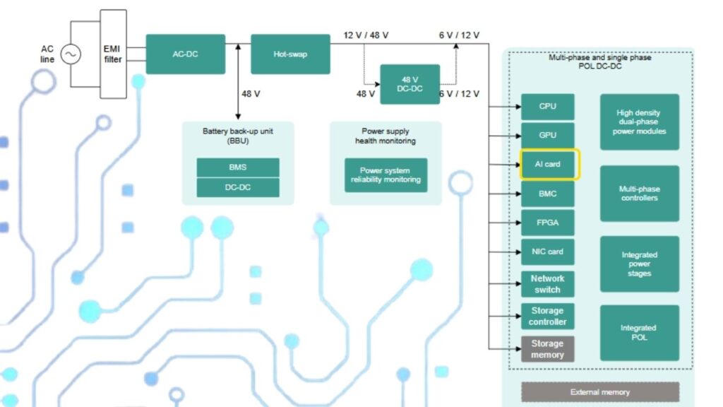
AI workloads are power-hungry and require efficient power conversion. Infineon’s ultra-thin wafers are already being used in Integrated Smart Power Stages (DC-DC converters), which feed power to CPUs, GPUs, and AI chips in data centers. These converters help manage the complex power needs of modern servers, which can contain up to $1,800 worth of power chips in the latest AI architectures.
Consumer Electronics and Motor Control
From laptops to electric vehicles, any device that needs efficient power management can benefit from thinner, more efficient wafers. The technology is expected to replace conventional wafers in low-voltage power converters within three to four years.
Industry and Manufacturing
Infineon’s innovation is already qualified and released to customers, with public demonstrations at major industry events like electronica 2024 in Munich.
The Future: Toward True 2D Silicon Electronics
While 20-micrometer wafers are a massive leap forward, the ultimate goal for many scientists is true 2D silicon materials—sheets just one atom thick, known as silicene. While silicene holds promise for even faster, more efficient electronics, it’s still in the research phase and not yet ready for mass production. Infineon’s breakthrough, however, brings us a big step closer to that future by pushing the boundaries of what’s possible with silicon today.
Step-by-Step Guide: How Ultra-Thin Silicon Wafers Are Made
1. Crystal Growth
High-purity silicon is grown into large, single-crystal ingots.
2. Wafer Slicing
The ingot is sliced into thin wafers, traditionally 40–60 µm, but now as thin as 20 µm with Infineon’s process.
3. Wafer Grinding & Polishing
Advanced grinding and polishing techniques are used to achieve the ultra-thin profile while maintaining strength and flatness.
4. Backside Metal Stacking
A metal layer is applied to connect the chip, requiring precise handling since it can be thicker than the wafer itself.
5. Quality Control
Wafers are tested for uniformity, strength, and electrical properties.
6. Integration into Devices
The wafers are then used to manufacture power devices like MOSFETs and integrated power stages for use in a wide range of electronics.
Tin-Based Pb-Free Perovskite Solar Cells Hit 16.65% Efficiency With 1500-Hour Stability
Researchers Develop Metallic Materials Using Data-Driven Frameworks and Explainable AI
FAQs About World’s Thinnest Silicon-Based Material
Q1: What is a silicon wafer?
A silicon wafer is a thin slice of silicon used as the base for building electronic circuits and devices.
Q2: Why is wafer thickness important?
Thinner wafers reduce electrical resistance, improve energy efficiency, and allow for more compact, powerful electronics.
Q3: How thin is 20 micrometers?
It’s about a quarter of the thickness of a human hair and half as thick as most wafers used today.
Q4: Where will I see this technology first?
In AI data centers, high-performance computing, and soon in consumer electronics like laptops and smartphones.
Q5: Is this technology available now?
Yes, Infineon has already released the technology to customers and is ramping up production.
Q6: How does this help the environment?
By making electronics more energy-efficient, it reduces overall power consumption and supports global sustainability goals.
