Phonon Wave Dynamics: Imagine a world where buildings can flex to absorb earthquakes, computers run faster with less heat, and robots are made from materials that change shape on command. This is not science fiction—it’s the future promised by metamaterials. And now, thanks to a groundbreaking discovery, scientists have taken a giant leap forward: they have directly observed phonon wave dynamics in self-assembling nanomaterials, unlocking an unprecedented level of control over these super-materials.

In this article, we’ll break down what this means, why it matters, and how it could change the world around us. Whether you’re a curious student, an engineer, or a business leader, you’ll find practical insights, clear examples, and expert guidance in plain language.
Phonon Wave Dynamics
| Aspect | Details |
|---|---|
| Discovery | First direct observation of phonon wave dynamics in self-assembling nanomaterials |
| Technique | Liquid-phase electron microscopy |
| Key Benefits | Customizable, reconfigurable metamaterials; improved shock absorption, energy guidance, and computing |
| Real-World Examples | Earthquake-resistant structures, deep-sea sponge skeletons, advanced computer chips |
| Research Leaders | University of Illinois Urbana-Champaign, University of Michigan, University of Wisconsin |
| Publication | Nature Materials |
| Official Resource | University of Illinois Newsroom |
The direct observation of phonon wave dynamics in self-assembling nanomaterials is a game-changer. It opens the door to customizable, reconfigurable metamaterials with applications limited only by our imagination. From safer buildings and smarter computers to advanced robots and medical devices, this discovery is set to transform technology and industry.
By understanding and harnessing the invisible “ripples” of energy inside materials, scientists are forging a future where matter itself can be programmed for any purpose. Stay tuned—this is just the beginning.
What Are Phonons and Metamaterials?
Understanding Phonons

Phonons are like invisible ripples of energy that travel through materials. Think of them as tiny packets of sound and vibration—much like how a pebble creates waves in a pond. These ripples move through the building blocks of matter, whether they are atoms, molecules, or even nanoparticles.
- Phonons help transfer heat, sound, and even the vibrations you feel during an earthquake.
- They are a quantum mechanical phenomenon, meaning they follow the strange rules of the atomic world.
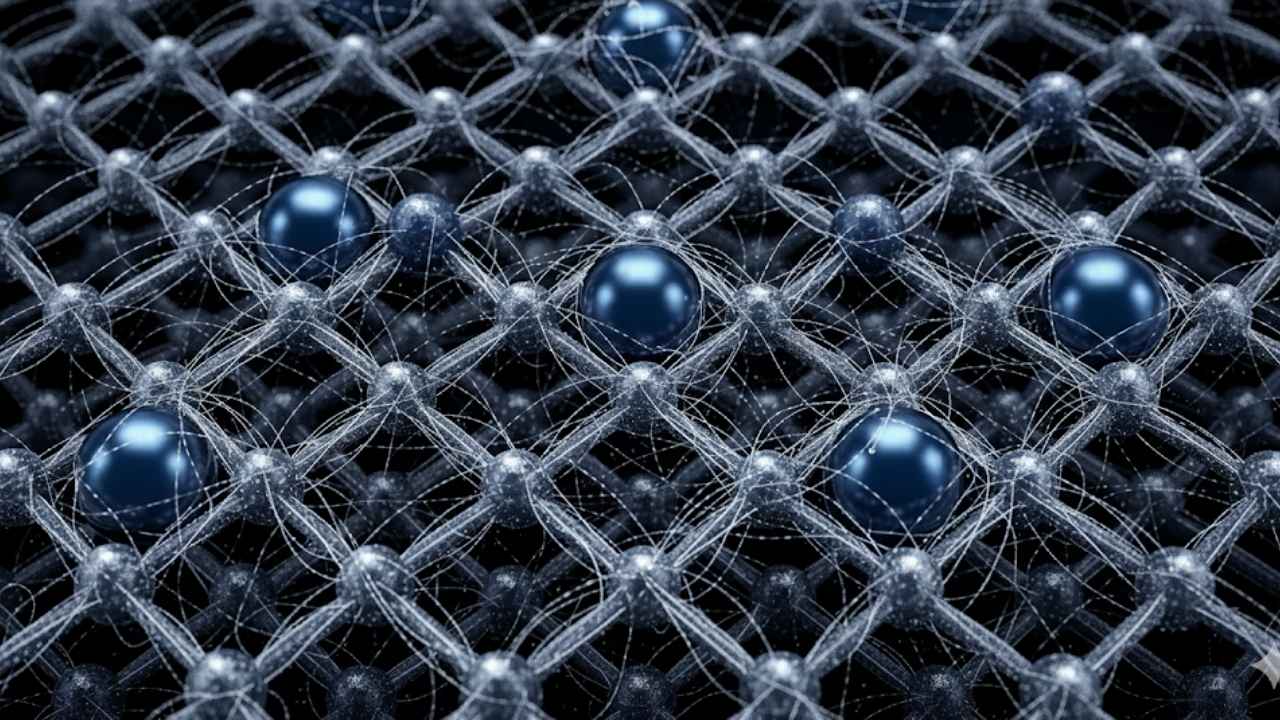
What Are Metamaterials?
Metamaterials are materials engineered to have properties that aren’t found in nature. Instead of relying on their chemical makeup, their special abilities come from their structure—how their tiny parts are arranged.
- Examples: Materials that bend light in unusual ways, absorb shocks, or guide sound and heat with precision.
- Self-assembling nanomaterials are tiny building blocks that organize themselves into larger, useful structures, much like LEGO bricks snapping together on their own.
Why Is Direct Observation of Phonon Dynamics a Big Deal?
Until now, scientists could only guess how phonons moved through these tiny, self-assembling materials. They used computer models and indirect measurements, but never saw the process in action. This was like trying to understand how a watch works by listening to its ticking, without ever opening it up.
That changed with the invention of a new technique: liquid-phase electron microscopy. This tool lets scientists see the actual movement of phonons as nanomaterials assemble themselves in real time.

- First time ever: Researchers watched phonon waves travel and interact inside self-assembling nanomaterials.
- New insights: They measured properties like phonon band structures (how energy moves), nanoscale spring constants (how stiff the material is), and deformation paths (how the material bends and stretches).
How Did Scientists Make This Discovery?
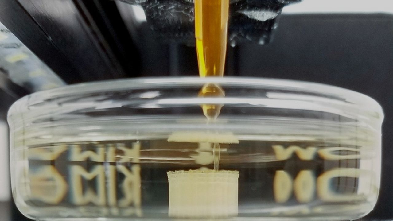
Step 1: Creating the Nanomaterials
Scientists started with nanoparticles—tiny particles a thousand times smaller than a human hair. These particles are designed to come together (self-assemble) into organized patterns, like a crystal or a honeycomb.
Step 2: Watching with Liquid-Phase Electron Microscopy
Using a special microscope, researchers watched these nanoparticles as they moved and joined together in a liquid environment. This allowed them to see the real-time “dance” of the particles and the phonon waves passing through them.

Step 3: Measuring the Phonon Dynamics
By analyzing the vibrations and movements, scientists could:
- Map out how energy travels through the material.
- See how the arrangement of particles changes the way phonons move.
- Understand how to design materials that can control energy flow in new ways.
Real-World Examples and Applications
Earthquake-Resistant Structures
Some buildings use metamaterials to redirect seismic waves, protecting them from earthquake damage. By controlling phonons, engineers can design structures that flex and absorb energy, rather than crack or collapse.
Nature’s Inspiration: Deep-Sea Sponges
The lightweight, yet tough skeletons of deep-sea sponges are natural examples of materials that guide phonons along specific paths. These structures help the sponges survive under crushing ocean pressure. Scientists are now mimicking these designs to create stronger, lighter materials.
Advanced Computing and Energy Devices
Metamaterials can guide heat and sound away from sensitive computer parts, making devices faster and more efficient. They can also be used in sensors, robots, and even medical devices that need to change shape or absorb shocks.
Practical Advice: How Will This Affect Your Life or Career?
For Students and Educators
- Learn the basics of quantum mechanics and material science—these fields are shaping the future of technology.
- Experiment with models: Use simple simulations or classroom experiments to visualize how waves move through different materials.
For Engineers and Scientists
- Stay updated: Follow advances in nanotechnology and metamaterials through reputable science journals and university newsrooms.
- Collaborate across fields: This research combines physics, chemistry, engineering, and computer science. Interdisciplinary teams are key to innovation.
For Business Leaders and Innovators
- Watch for new products: The ability to design materials with custom properties will impact industries from construction to electronics and healthcare.
- Invest in R&D: Companies that support research in nanomaterials and metamaterials are likely to lead in next-generation products.
Step-by-Step Guide: How to Understand and Use This Discovery
Step 1: Grasp the Basics
- Know what phonons and metamaterials are.
- Understand why controlling energy flow at the nanoscale is valuable.
Step 2: Follow the Research
- Read summaries and articles from trusted university newsrooms and leading science publications.
Step 3: Think About Applications
- How could materials that absorb shocks or guide energy be used in your field?
- What problems could be solved with materials that change shape or properties on demand?
Step 4: Explore Further Learning
- Take online courses in nanotechnology, quantum mechanics, or material science.
- Attend conferences or webinars on metamaterials and advanced manufacturing.
Quantum Photonic Interconnects via Nanofibers Advance Distributed Quantum Architecture
Photonic Nanofabrication Enables Miniaturized Neutral Atom Quantum Networking
DNA Enabled Nanostructures Proposed To Achieve Superradiance For Quantum Light Sources
FAQs About Phonon Wave Dynamics
What is a phonon, in simple terms?
A phonon is a tiny packet of vibration or sound energy that moves through a material, like a ripple in water or a sound wave in air.
Why are metamaterials important?
They let us create materials with special abilities—like bending light, absorbing shocks, or guiding heat—that natural materials can’t do on their own.
How does this discovery help?
By directly observing phonons in self-assembling nanomaterials, scientists can design materials with custom properties for use in buildings, electronics, and more.
What industries will benefit most?
Construction (earthquake-resistant buildings), electronics (better cooling and energy flow), robotics, aerospace, and healthcare are just a few examples.