QuantumDiamonds Launches Diamond-Based Microscopy Tool: The world of semiconductors just got a little bit brighter—and a lot more precise. QuantumDiamonds GmbH has unveiled the QD m.0, the world’s first commercial quantum device specifically designed for semiconductor chip failure analysis using diamond-based quantum microscopy. This breakthrough is set to revolutionize how engineers and manufacturers detect, locate, and fix tiny but costly faults in the microchips that power our smartphones, computers, cars, and even satellites.
Imagine trying to find a single grain of sand hidden inside a multi-layered cake. Now, imagine that cake is the size of your fingernail, and the grain of sand is a microscopic defect that could ruin the whole dessert. That’s the kind of challenge the semiconductor industry faces every day. With chips getting smaller, faster, and more complex, traditional tools are struggling to keep up. That’s where QuantumDiamonds steps in, offering a new way to “see” inside chips with incredible accuracy.
QuantumDiamonds Launches Diamond-Based Microscopy Tool
| Feature/Statistic | Details |
|---|---|
| Product Name | QD m.0 |
| Company | QuantumDiamonds GmbH |
| Technology | Diamond-based quantum microscopy |
| Key Capability | Detects and localizes faults in integrated circuits with unprecedented precision |
| Target Industry | Semiconductor manufacturing |
| Relevance | 2.5D/3D packaging, chiplet-based architectures, advanced packaging |
| Delivery | First batch shipped Q4 2024 |
| Allocation | Initial run fully allocated |
| Official Website | QuantumDiamonds GmbH (for more info) |
| Professional Impact | Improves production yields, reduces defect rates, accelerates chip production ramp-up |
The launch of the QD m.0 by QuantumDiamonds GmbH marks a major leap forward for the semiconductor industry. By harnessing the power of diamond-based quantum microscopy, this innovative tool helps engineers find and fix faults in chips with unprecedented precision, speed, and ease. Whether you’re a seasoned professional or just curious about how our gadgets work, the QD m.0 is a shining example of how science and technology can solve real-world problems.
What Is Diamond-Based Quantum Microscopy?
Diamond-based quantum microscopy is a cutting-edge technique that uses tiny defects inside diamonds—called nitrogen-vacancy (NV) centers—to detect and measure magnetic fields with extreme sensitivity. Think of it as a super-powered microscope that can “see” not just shapes and colors, but also invisible magnetic signals coming from tiny electrical currents inside chips. This allows engineers to find faults that are otherwise impossible to detect with regular microscopes.
How does it work?
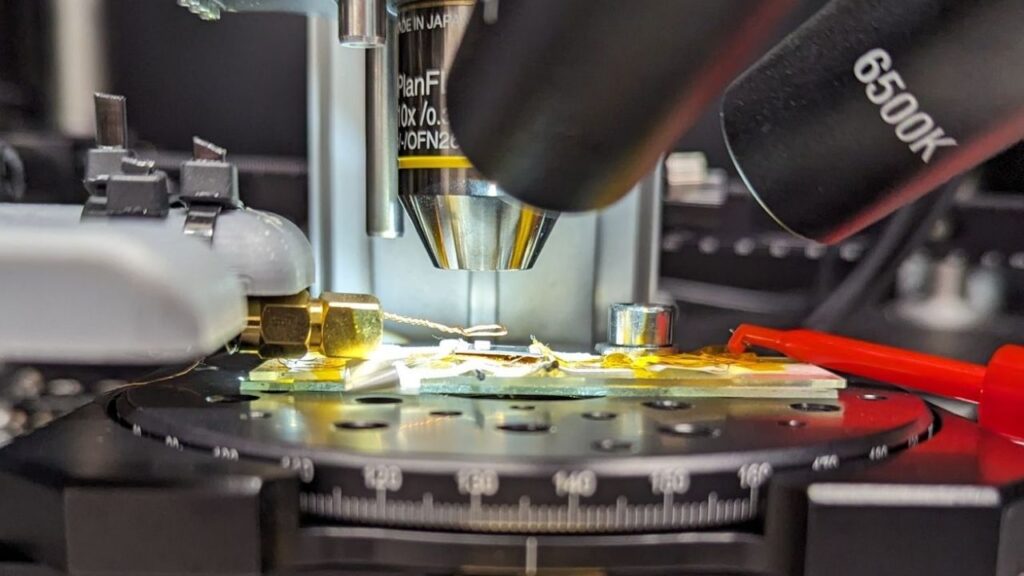
When a chip is powered up, tiny electrical currents flow through its circuits. These currents create magnetic fields. The diamond sensor in the QD m.0 picks up these magnetic fields and turns them into detailed maps, showing exactly where something might be wrong—even if the fault is buried deep inside multiple layers of the chip.
Why Is This Important for the Semiconductor Industry?
Semiconductors are the brains of almost every electronic device. As technology advances, chips are becoming more complex, with multiple layers (like a stack of pancakes) and tiny connections between them. This is called heterogeneous integration and includes techniques like die-stacking, through-silicon vias, hybrid bonding, and advanced packaging.
When something goes wrong in these complex chips, it’s like trying to find a needle in a haystack. Traditional tools can’t always find the problem, leading to lower production yields and higher costs. The QD m.0 changes this by providing unprecedented precision in detecting and localizing faults, helping manufacturers improve quality and save millions of dollars.
How Does the QD m.0 Compare to Traditional Tools?
To understand why the QD m.0 is special, let’s compare it to traditional failure analysis tools:
| Feature | Traditional Tools | QD m.0 (Diamond-Based Microscopy) |
|---|---|---|
| Detection Method | Optical/electron microscopy, probing | Quantum magnetic field sensing |
| Spatial Resolution | Limited by wavelength/beam size | Less than 1 micron (super sharp!) |
| Layer Penetration | Surface or limited depth | Multiple layers, non-destructive |
| Speed | Slow, often destructive | Fast, non-destructive |
| Complexity | Needs special sample prep, vacuum, etc. | Works at room temperature, no special prep |
The QD m.0 stands out because it can detect faults across multiple layers without damaging the chip, and it does this with high speed and accuracy.

A Step-by-Step Guide: How QD m.0 Helps Find Chip Faults
Let’s break down how the QD m.0 is used to find and fix chip problems:
- Prepare the Chip
The chip is placed under the microscope. No special preparation is needed—just power it up! - Scan with Diamond Sensor
The diamond sensor scans the chip, picking up magnetic signals from electrical currents flowing inside. - Create a Magnetic Map
The QD m.0 creates a detailed map of the magnetic fields, showing exactly where currents are flowing—or not flowing, if there’s a fault. - Identify Faults
Engineers look at the map to find unusual patterns or missing signals, indicating a fault. - Localize the Problem
The QD m.0 pinpoints the exact location of the fault, even if it’s buried deep inside the chip. - Fix and Improve
With the problem identified, engineers can fix the chip or improve the manufacturing process to prevent future faults.
Real-World Example: Solving a Mystery Inside a Smartphone Chip
Imagine a smartphone that keeps crashing. Engineers suspect a fault in the processor chip, but traditional tools can’t find it. Using the QD m.0, they scan the chip and discover a tiny break in a connection deep inside a 3D stack. With this information, they can fix the design or manufacturing process, making future chips more reliable.
Practical Advice for Engineers and Manufacturers
- Embrace New Technology: Don’t be afraid to try advanced tools like the QD m.0. They can save time and money in the long run.
- Focus on Yield: Even a small improvement in yield can mean big savings for large-scale production.
- Collaborate: Work with partners like QuantumDiamonds to stay ahead of the curve in chip manufacturing.
The Science Behind the Magic
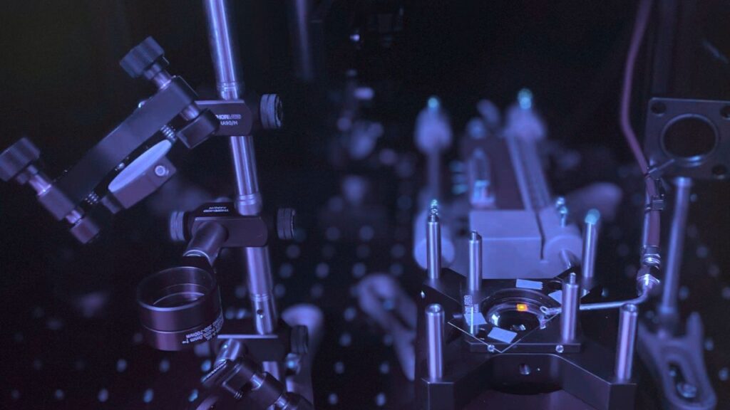
At the heart of the QD m.0 is the nitrogen-vacancy (NV) center in diamond. These NV centers are tiny defects that can sense magnetic fields with incredible sensitivity. When a laser shines on the diamond, the NV centers glow in a way that changes depending on the magnetic field around them. By measuring this glow, the QD m.0 can create a map of magnetic fields inside a chip.
No special conditions are needed—the QD m.0 works at room temperature and doesn’t require vacuum or cryogenic cooling, making it easy to use in any lab.
Who Benefits from the QD m.0?
- Semiconductor Manufacturers: Improve yield, reduce defects, and speed up production.
- Chip Designers: Get detailed feedback on how well new designs work.
- Failure Analysis Engineers: Find and fix problems faster and more accurately.
- Research Labs: Explore new materials and chip architectures with confidence.
Quantum‑Centric Supercomputing Collaboration Begins Between IBM And Pasqal
Breakthrough in Electron Microscopy Captures Individual Nanoparticles with Unprecedented Precision
FAQs About QuantumDiamonds Launches Diamond-Based Microscopy Tool
Q: What is diamond-based quantum microscopy?
A: It’s a technique that uses special diamonds with NV centers to detect and measure magnetic fields with extreme precision, allowing engineers to find faults in chips that are invisible to other methods.
Q: Why is the QD m.0 better than traditional tools?
A: The QD m.0 can detect faults across multiple layers of a chip, works quickly and non-destructively, and doesn’t require special conditions like vacuum or cooling.
Q: How does the QD m.0 help save money?
A: By finding and fixing faults early, manufacturers can improve yield, reduce waste, and get new chips to market faster.
Q: Can the QD m.0 be used for other applications?
A: While designed for semiconductors, the technology could be adapted for other fields that need precise magnetic field sensing, such as materials science or biomedical imaging.
Q: Where can I learn more about the QD m.0?
A: Visit the official QuantumDiamonds GmbH website (see the table above).
