Could Trilayer Graphene’s Unusually High Kinetic Inductance Revolutionize Nanoelectronics?: Imagine a material so thin it’s just a few atoms thick, but powerful enough to change how we build tomorrow’s computers. That’s the promise of twisted trilayer graphene—a special arrangement of carbon sheets that’s making headlines for its unusually high kinetic inductance. This discovery could be a game-changer for nanoelectronics, especially in fields like quantum computing and advanced sensors.
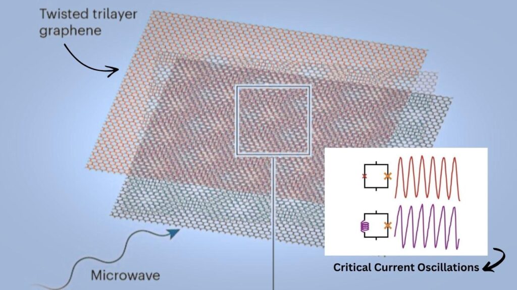
To put it simply, kinetic inductance is a property that describes how hard it is to push supercurrent (electric current with zero resistance) through a material. In regular metals or superconductors, this value is usually very small. But in magic-angle twisted trilayer graphene, researchers have found kinetic inductance values up to 150 nanohenries per square—that’s nearly fifty times higher than in traditional superconductors. Why does this matter? Because higher kinetic inductance means we can make super-sensitive sensors and new kinds of circuits that were impossible before.
Could Trilayer Graphene’s Unusually High Kinetic Inductance Revolutionize Nanoelectronics?
| Feature | Value/Insight | Professional/Career Insight |
|---|---|---|
| Kinetic Inductance | Up to 150 nH/□ (nanohenries per square) | Enables new quantum circuits |
| Comparison to Standard SCs | 50x higher than typical superconductors | Competitive edge for research teams |
| Tunability | Adjustable via electric field or doping | Engineers can fine-tune devices |
| Quantum Coherence | High, robust quantum states | Quantum computing applications |
| Superconducting Weak Link | Used in SQUIDs for sensitive measurements | Quantum sensors, metrology |
| Scalability | Challenging, but complements existing tech | Research focus for industry |
Twisted trilayer graphene’s unusually high kinetic inductance is opening new doors in nanoelectronics. With values up to 150 nanohenries per square and the ability to tune its properties with an electric field, this material could revolutionize quantum computing, sensors, and flexible electronics. While there are challenges to overcome, the future looks bright for this cutting-edge technology.
What Is Trilayer Graphene and How Is It Made?
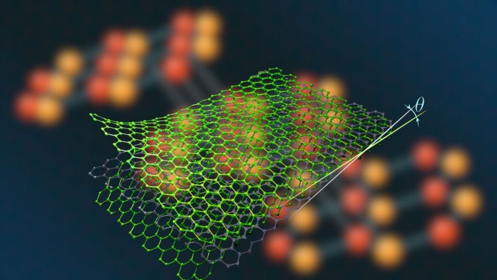
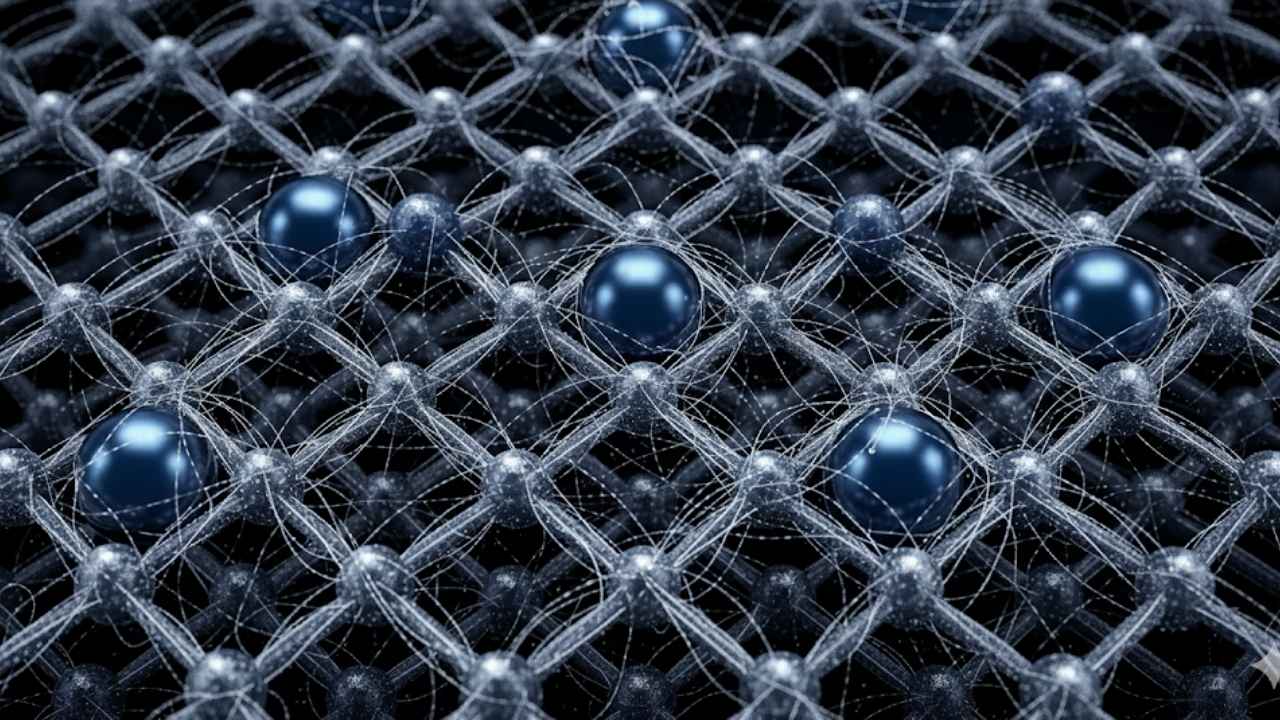
Trilayer graphene is exactly what it sounds like: three sheets of carbon atoms, each arranged in a honeycomb pattern. But the real magic happens when scientists twist the middle layer at a specific “magic angle”—about 1.7 degrees—relative to the top and bottom layers. This twist changes how electrons move, opening the door to superconductivity (where electricity flows with zero resistance) and other exotic behaviors.
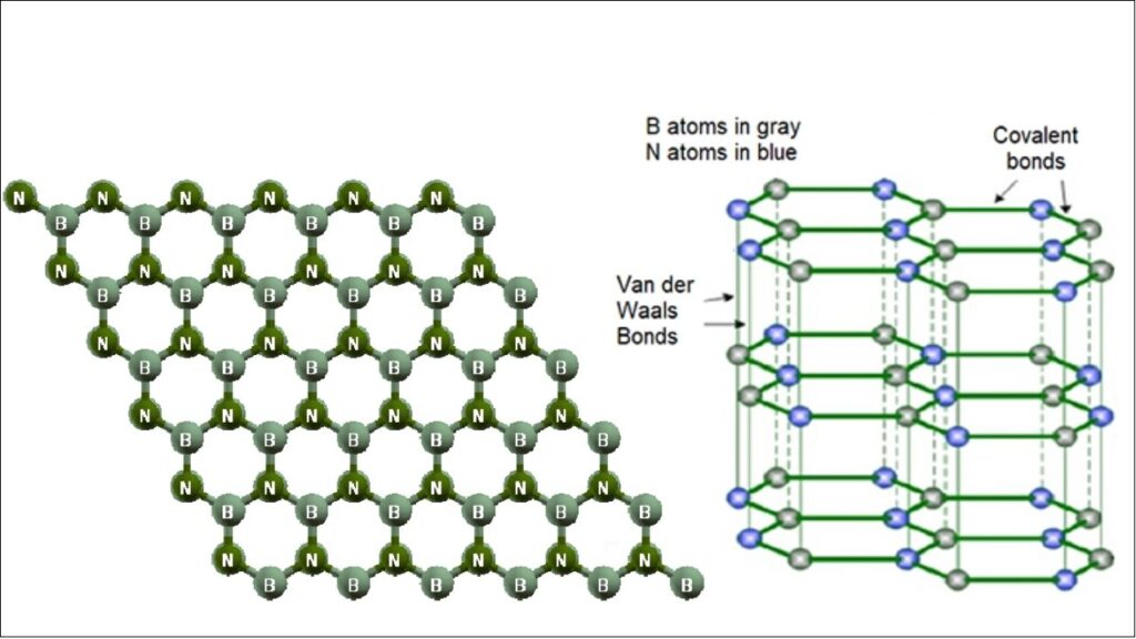
To build a device, scientists sandwich the twisted trilayer graphene between layers of hexagonal boron nitride (hBN), which protects the delicate structure. Then, they add electrodes above and below to control the electric field and fine-tune the material’s properties. This process is complex, but it’s worth it for the amazing results.
What Is Kinetic Inductance and Why Is It Important?
Let’s break it down:
- Inductance is like the “inertia” of electricity—it’s how much a material resists changes in current.
- Kinetic inductance comes from the movement (kinetics) of paired electrons (called Cooper pairs) in superconductors.
- High kinetic inductance means it’s harder to push current through, but it also means we can make much more sensitive circuits.
In everyday electronics, we use regular inductors (coils of wire) to store energy or filter signals. But in nanoelectronics, especially for quantum devices, we need something much smaller and more precise. That’s where twisted trilayer graphene shines—its high kinetic inductance lets us build tiny, powerful circuits that can sense things like magnetic fields with incredible accuracy.
How Scientists Measure and Use Kinetic Inductance
Researchers use special devices called superconducting quantum interference devices (SQUIDs) to study these materials. A SQUID is like a super-sensitive compass for magnetic fields. In their experiments, scientists interrupted a loop of superconducting wire with two “weak links” made of twisted trilayer graphene.
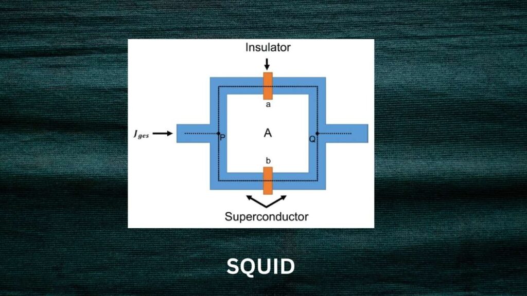
By applying electric fields and measuring how the current changes, they found that the kinetic inductance could be tuned by adjusting the voltage—making the material incredibly versatile. This tunability is a big deal for engineers, who can now design circuits that adapt to different tasks.
Practical Examples: What Can Trilayer Graphene Do?
Here are some real-world applications:
- Quantum Sensors: With its high kinetic inductance, trilayer graphene can detect tiny changes in magnetic fields—useful for medical imaging, mineral exploration, and even studying the brain.
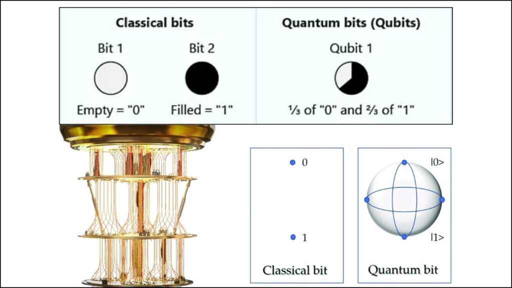
- Quantum Computers: These materials could help build the next generation of quantum bits (qubits), which need to be both stable and sensitive.
- Tunable Circuits: Engineers can adjust the properties of these circuits on the fly, opening up new possibilities for flexible electronics.
Step-by-Step Guide: How Does This Technology Work?
Let’s walk through the process, step by step:
- Prepare the Layers: Stack three sheets of graphene, twisting the middle layer at the magic angle.
- Protect the Structure: Sandwich the graphene between hBN layers to keep it stable.
- Add Electrodes: Place electrodes above and below to control the electric field.
- Test in a SQUID: Insert the graphene as a “weak link” in a superconducting loop.
- Measure and Tune: Apply different voltages and measure how the current flows.
- Analyze the Data: Calculate the kinetic inductance and see how it changes with the electric field.
Challenges and Future Prospects
While the potential is huge, there are still challenges:
- Scalability: Making large sheets of twisted trilayer graphene is tricky, and integrating them into mass-produced devices is even harder.
- Integration: These materials need to work with existing electronics, which means developing new fabrication techniques.
- Cost: The process is currently expensive, but as technology improves, costs are expected to come down.
Despite these hurdles, researchers are optimistic. Twisted trilayer graphene could complement existing technologies, making new kinds of sensors and circuits possible.
China Uses Quantum Computer to Break RSA Encryption—A Wake-Up Call for Global Cybersecurity
Superconducting Magnets Detect Gravitational Waves—A New Way to Observe the Universe
World’s First Silicon-Free Computer Built With 2D Materials—A Major Shift Begins at Penn State
FAQs About Could Trilayer Graphene’s Unusually High Kinetic Inductance Revolutionize Nanoelectronics?
Q: What is twisted trilayer graphene?
A: It’s three layers of carbon atoms arranged in a honeycomb pattern, with the middle layer twisted at a specific angle to create unique electronic properties.
Q: What is kinetic inductance?
A: It’s a property that describes how hard it is to push supercurrent through a material, arising from the inertia of paired electrons in superconductors.
Q: Why is high kinetic inductance important?
A: It allows for the creation of ultra-sensitive sensors and new types of circuits, especially in quantum technologies.
Q: Can this technology be used in everyday electronics?
A: Not yet, but it has huge potential for quantum computers, sensors, and advanced electronics in the future.
Q: What are the main challenges?
A: Making large, high-quality sheets and integrating them into existing devices is difficult and expensive.
