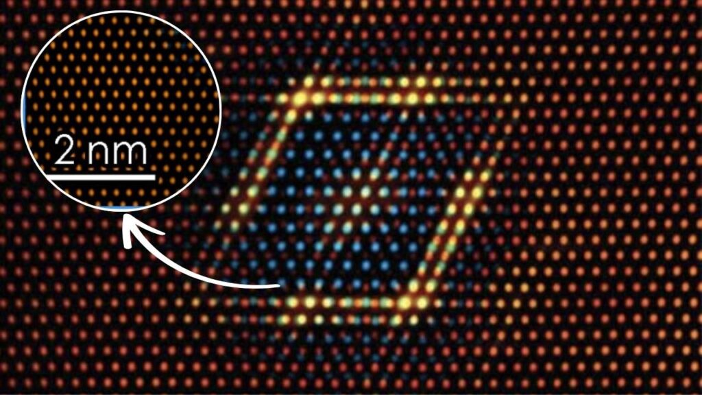
Imagine being able to carve or build incredibly tiny copper structures so small you can’t see them with a regular microscope. Thanks to a pioneering technology developed by researchers at the Georgia Institute of Technology, this is now possible. A specially focused electron beam can both etch away and deposit copper atoms at the nanoscale — down to about 50 nanometers (about 1/2000th the width of a human hair) or even smaller, with atomic-level precision.

This breakthrough technique is set to transform the electronics industry by enabling ultra-miniaturized devices, quantum computers, high-precision sensors, and more. In this article, we will break down how this technology works, why it is so important, and its far-reaching applications — presented clearly for beginners and with sufficient depth for professionals.
Table of Contents
What is Electron Beam Nanoscale Copper Sculpting?
Electron beam nanoscale copper sculpting is an innovative fabrication technique that lets scientists use a focused electron beam — essentially a tiny, highly energetic stream of electrons — to both remove (etch) and add (deposit) copper atoms on a surface. Unlike previous methods that could either etch or deposit but not both in one process, this new method allows dynamic switching between these two modes within the same experimental setup.
Why is Copper Important?
Copper is indispensable in electronics because of its excellent electrical conductivity, thermal conductivity, and ductility. It is the primary material for wiring and interconnects inside microchips and electronic devices. Controlling copper structures at the nanoscale enables fabrication of advanced electronic components that are smaller, faster, and more energy-efficient, key to the progress in computing, telecommunications, and sensors.
How Does This Electron Beam Sculpting Work? — A Closer Look
1. The Liquid Chemical Environment: Copper in Water-Ammonia Solution
The process takes place inside a carefully controlled liquid environment composed of water mixed with ammonia. This solution surrounds the copper substrate (the base material to be sculpted). The unique chemistry of this environment allows the electron beam to perform different tasks depending on the concentration of ammonia:
- At low ammonia concentrations, the beam etches copper atoms off the surface.
- At higher ammonia concentrations, the beam deposits copper atoms onto the surface, building up tiny structures.
This chemical control is crucial because it lets the electron beam act as both a nanoscale “scalpel” and a “pen” for copper.

2. Electron Beam Dynamics: The ‘Sculptor’ Tool
The electron beam is generated inside an electron microscope and is focused down to diameters of just a few nanometers. When electrons hit the copper surface immersed in the liquid environment, they interact with copper atoms and the nearby water-ammonia molecules to trigger chemical reactions:
- Etching mode: Low ammonia promotes oxidation of copper atoms at the surface, making them detach and dissolve.
- Deposition mode: Higher ammonia enables a chemical reduction that causes copper ions in solution to deposit onto the surface in precise locations under the beam.
3. High Precision and Dynamic Mode Switching
By controlling parameters such as:
- Electron dose (number of electrons delivered per area),
- Exposure time,
- Beam scanning pattern and speed,
- Ammonia concentration in the liquid,
researchers can sculpt copper structures with remarkable accuracy. The ability to switch dynamically between etching and deposition by adjusting the local chemical environment allows for complex 3D nanoscale fabrication. This reduces manufacturing steps and enables intricate patterning impossible with conventional top-down lithography.
Electron Beams Now Sculpt Copper at the Nanoscale
| Highlight | Details |
|---|---|
| Technology Developer | Georgia Institute of Technology, Professor Andrei Fedorov |
| Material Sculpted | Copper at nanoscale (down to atomic precision, ~50 nm features) |
| Process Environment | Liquid water-ammonia solution controlling etching or deposition |
| Precision Scale | Patterns as small as tens of nanometers, approaching atomic scale |
| Process Modes | Both additive (deposition) and subtractive (etching) combined dynamically |
| Key Chemical Role | Ammonia concentration governs copper atom removal or buildup |
| Advantage Over Existing Tech | Combines etching and deposition in one system; supports 3D structuring with atomic resolution |
| Potential Applications | Next-generation electronics, quantum computers, nanosensors, 3D circuits |
| Publication Year | 2025 |
| Official Source | Georgia Tech Woodruff School of Mechanical Engineering |
The breakthrough in electron beam nanoscale copper sculpting developed by Georgia Tech researchers represents a major leap forward in nanotechnology and electronics manufacturing. By enabling atomic-scale precise, 3D copper nanostructures through a single versatile process that both etches and deposits, this technique opens the door to revolutionary advances in electronics, quantum devices, sensing technologies, and more.
As this technology matures, it promises to help overcome the challenges of miniaturization and complexity that traditional fabrication techniques face. The future of electronics—smaller, faster, more powerful, and quantum-enabled—is being shaped, quite literally, at the atomic level.
Why This Discovery Is a Game-Changer for Electronics and Nanotechnology
Advancing Miniaturization and Circuit Complexity
Traditional semiconductor manufacturing uses photolithography, which is increasingly challenged by physical limits as feature sizes approach atomic dimensions. This breakthrough moves beyond those limits by enabling direct 3D sculpting of copper nanostructures at atomic scales, offering:
- Greater density of wiring and components,
- Reduced electrical resistance via high-purity copper paths,
- Ability to create truly 3-dimensional nanoscale circuit architectures.
Enabling Quantum Nanotechnology
Quantum computing and sensing devices rely on nanoscale precision to manipulate quantum states without disturbance. This beam sculpting method promises fabrication of components such as:
- Ultra-fine wiring for qubits,
- Nanosensors detecting single molecules or spins,
- Complex 3D structures designed to maintain quantum coherence.

Flexible and Cost-Effective Manufacturing
Combining additive and subtractive fabrication in one process significantly reduces equipment complexity and cycle time. This enhances flexibility, lowers costs, and potentially scales nanomanufacturing beyond conventional clean room requirements.
Step-by-Step Guide to the Electron Beam Copper Sculpting Process
Step 1: Setting Up the Chemical Environment
- A copper substrate is immersed in a controlled mixture of water and ammonia.
- Ammonia concentration is carefully set and monitored.
- The solution provides a stable environment for copper ion chemistry and electron interactions.
Step 2: Focusing the Electron Beam
- Using a scanning transmission electron microscope (STEM), the electron beam is focused to nanometer diameters.
- Operators program the beam path and dose to define shapes.
Step 3: Controlled Etching and Deposition
- At different points on the substrate, ammonia concentration or beam parameters are changed to switch between etching or deposition.
- This lets the creation of trenches, peaks, and complex 3D forms by combining subtractive and additive steps.
Step 4: Real-Time Monitoring and Refinement
- High-resolution imaging ensures structures adhere to design.
- Adjustments are made to beam intensity or solution chemistry for optimal results.
- The process occurs inside the microscope chamber allowing immediate feedback.
Practical Examples of Applications
- Microelectronics: Creating ultra-fine copper interconnects for processors and memory chips, enabling faster, smaller, energy-efficient electronics.
- Quantum Devices: Fabricating 3D wiring and control structures necessary for qubit arrays and quantum sensors.
- Biomedical Sensors: Building nanoscale probes capable of detecting specific biomolecules or delivering drugs with high accuracy.
- Energy Technologies: Developing nanoscale copper electrodes for batteries and capacitors with enhanced charge transport.
New Copper Alloy Works in −200 °C Temps — Designed for Space, and It Remembers Its Shape
Scientists Develop Breakthrough Copper Composite With Superior Strength and Conductivity
New Light Phenomenon Found in Common Gypsum: A Scientific Breakthrough Explained for Everyone
FAQs About Electron Beams Now Sculpt Copper at the Nanoscale
Q1: What feature sizes can be achieved?
This technique can reliably sculpt copper features down to approximately 50 nanometers or smaller, with potential for atomic-level resolution depending on process optimization.
Q2: How does ammonia affect etching versus deposition?
Ammonia concentration changes the solution’s chemical equilibrium:
- Low ammonia enhances copper oxidation and removal (etching).
- Higher ammonia levels promote copper ion reduction and deposition.
Q3: Is copper purity maintained?
Yes, the process results in high-purity copper structures because the electron beam induces localized chemical reactions without introducing significant contamination.
Q4: Can the method be extended to other metals?
Researchers are investigating other metals; while copper is currently the focus, the general approach of electron beam-induced chemical effects in liquid environments is adaptable.
Q5: How does this compare with traditional lithography?
Unlike lithography, which is mostly 2D and involves masks and multiple steps, this method supports direct-write, additive plus subtractive 3D nanosculpting with atomic precision, eliminating mask costs and complexity.