Understanding the tiny world of atoms can unlock vast potential for technology, especially in electronics. A new AI-powered tool called IsoDAT2D is transforming how scientists study ultra-thin films — materials just thousands of times thinner than a human hair that are essential for devices like smartphones, computers, and wearable tech. Developed by University of Florida engineering professor Megan Butala and her team, IsoDAT2D uses machine learning to decode the atomic structure of these films, overcoming traditional challenges and opening exciting possibilities for faster, smarter, and more energy-efficient electronics.

Ultra-thin films are the building blocks of computer chips and other semiconductor devices. Yet, precisely understanding their atomic arrangement has been notoriously difficult because these films rest on much thicker single-crystal substrates, whose signals overshadow the film’s atomic signatures during measurement. IsoDAT2D overcomes this obstacle by cleverly separating the tiny atomic “fingerprints” of the films from the dominant substrate signals using advanced AI algorithms.
Here’s a comprehensive and expanded guide to this breakthrough, its significance, and how it’s poised to revolutionize materials science and technology.
Table of Contents
AI Tool Reveals Atomic Secrets of Ultra-Thin Films
| Key Aspects | Details |
|---|---|
| Tool Name | IsoDAT2D |
| Developed By | Prof. Megan Butala and team, University of Florida Department of Materials Science & Engineering |
| Technology Used | Machine learning: Non-negative matrix factorization (NMF), Hierarchical agglomerative clustering (HAC) |
| Application | Revealing atomic structure of ultra-thin films on single-crystal substrates |
| Film Examples | Silicon dioxide, metal nitrides (used in semiconductors) |
| Thickness of Films | Thousands of times thinner than human hair |
| Benefits | Accelerates material design, enables precise semiconductor manufacturing, improves energy efficiency |
| Data Source | 2D X-ray total scattering data |
| Official Research Publication Link | University of Florida Department of Materials Science & Engineering |
IsoDAT2D represents a transformative leap in materials science by providing a powerful, AI-driven lens into the atomic structures of ultra-thin films crucial for modern electronics. This breakthrough accelerates the design of faster, smaller, and more energy-efficient semiconductor devices that are foundational to the technologies shaping our daily lives.
By bridging advanced X-ray scattering with machine learning, IsoDAT2D empowers scientists and engineers to innovate with unprecedented precision and confidence. As this tool gains broader adoption, it promises to unlock new frontiers in electronics, energy, and quantum materials, truly ushering in a new era of materials discovery.
What Are Ultra-Thin Films and Why Are They Important?
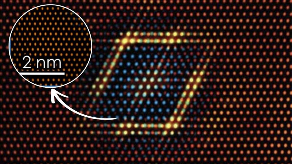
Ultra-thin films are incredibly thin layers of material, typically a few nanometers thick — that’s thousands of times thinner than a human hair. Despite their tiny size, these films play critical roles in many technologies. They are used in electronics as coatings, insulators, conductors, and active functional layers in devices like computer chips, sensors, and energy storage systems.

Because of their small size, even minute variations in the atomic arrangement within these films can cause significant changes in the material’s electrical, thermal, optical, and mechanical properties. For example, in semiconductor chips, how atoms are arranged impacts the chip’s speed, energy consumption, and reliability.
That’s why scientists have long sought a detailed understanding of the atomic structure of ultra-thin films — knowledge that is essential to design materials with tailor-made properties for advanced tech applications.
The Challenge: Seeing the Atomic Structure of Ultra-Thin Films
Traditional methods to study atomic structures, like X-ray scattering, rely on measuring how X-rays bounce off a material’s atoms. While effective for thick samples, this method hits a serious roadblock when used on ultra-thin films resting on single-crystal substrates (like silicon wafers).

The substrate, much thicker than the film, generates strong X-ray scattering signals that overwhelm the much weaker signals from the thin film itself.
This “signal overshadowing” makes it extremely difficult to isolate the atomic information of the ultra-thin film, limiting scientists’ ability to precisely characterize it. Existing methods to separate signals either degrade data quality or demand complex experimental setups, further complicating research.
How IsoDAT2D Works: When Artificial Intelligence Meets Materials Science

IsoDAT2D is a novel solution leveraging machine learning and advanced data processing to overcome the signal overshadowing problem. Here’s an easy-to-follow breakdown of how it works:
- Data Collection with 2D X-ray Scattering
Scientists collect high-resolution 2D X-ray scattering data of ultra-thin films on substrates. Unlike compressing this rich data into a single summary graph, IsoDAT2D analyzes the full 2D image to capture more detailed structural variation. - Rotation and Integration
The 2D scattering images are sliced along multiple lines at different angles, creating many 1D patterns that reveal subtle differences in scattering information. - Advanced Machine Learning Algorithms
- Non-Negative Matrix Factorization (NMF): This technique breaks the complex data into separate source components, distinguishing between patterns generated by the thin film and those from the substrate.
- Hierarchical Agglomerative Clustering (HAC): Groups together similar components identified by NMF, further refining the isolation of the thin film’s unique atomic fingerprint.
- Signal Isolation and Noise Reduction
These algorithms filter out the substrate’s overpowering signal and random noise, resulting in clean scattering data representing only the thin film’s atomic arrangement. - Atomic Structure Determination
Using this refined data, scientists compute pair distribution functions (PDFs) — mathematical models that reveal atom-to-atom distances and arrangements. PDFs provide a 3D picture of how atoms are organized in the thin film with unprecedented clarity. - Designing Better Materials
Researchers can then use these precise atomic details to tailor thin film properties by adjusting composition, thickness, and processing conditions, leading to improved electronics and materials.
Unlike earlier methods, IsoDAT2D does not require specialized setups and preserves data quality, making atomic structure studies more accessible and reliable.
Why This Breakthrough Matters
Accelerating Materials Innovation
With clear atomic-level knowledge, materials scientists can drastically reduce trial and error in designing thin films. This leads to:
- Faster development cycles for new semiconductor components.
- Precise tuning of electrical and thermal properties.
- Enhanced materials for energy storage and smart sensors.
Enabling Smarter, Energy-Efficient Electronics
Better atomic understanding means chips can be made smaller, faster, and more efficient — powering everything from smartphones and laptops to wearable devices and AI applications.
Improving Research Reproducibility and Collaboration
IsoDAT2D’s computational workflow standardizes thin film analysis, making results more reproducible and comparable across labs worldwide. It also encourages sharing of data and software tools, fostering innovation.
Expanding Applications to Emerging Technologies
The tool’s ability extends beyond silicon-based films to complex materials such as metal nitrides, oxides, and novel composites used in:
- Quantum computing components
- Advanced battery electrodes
- Next-gen photonics and optoelectronics
Practical Example: Revolutionizing Chip Manufacturing
Modern semiconductor chips contain multiple ultra-thin films stacked layer by layer, each just a few atoms thick. The precise atomic structure of these layers determines chip performance.
Using IsoDAT2D, chip makers can:
- Detect atomic-scale defects or irregularities that impair performance.
- Optimize deposition and fabrication techniques for uniform films.
- Predict how design changes impact electrical conductivity and heat dissipation.
- Reduce manufacturing costs by minimizing trial-and-error experimentation.
- Develop chips that run cooler and last longer.
This translates into more reliable devices with improved processing speeds and energy efficiency, benefiting consumers and industry alike.
Step-By-Step Guide to Using IsoDAT2D in Research
- Prepare the Sample: Deposit ultra-thin films (silicon dioxide, metal nitrides, etc.) on single-crystal substrates like silicon wafers.
- Collect 2D X-ray Scattering Data: Use synchrotron or lab-based X-ray diffractometers to capture high-resolution scattering images.
- Process Data with IsoDAT2D: Run rotation-integration to convert 2D images into multiple 1D scattering profiles.
- Apply Machine Learning: Use Non-Negative Matrix Factorization and Hierarchical Agglomerative Clustering to separate film signals from substrate signals.
- Clean and Analyze Data: Smooth isolated signals and generate Pair Distribution Functions to interpret atomic arrangements.
- Interpret and Validate Structure: Understand atom-to-atom distances and refine models to match experimental data.
- Apply Insights to Material Design: Adjust processing conditions and film composition based on atomic insights to achieve desired properties.
New Quantum Material Reveals Hidden Metallic State for Ultra-Fast Electronics
World’s First Silicon-Free Computer Built With 2D Materials—A Major Shift Begins at Penn State
FAQs About AI Tool Reveals Atomic Secrets of Ultra-Thin Films
Q1: What makes IsoDAT2D better than traditional X-ray scattering methods?
Unlike classical methods, IsoDAT2D uses AI to cleanly separate weak thin film signals from strong substrate backgrounds without sacrificing data quality or requiring complex setups.
Q2: How thin are these ultra-thin films?
They typically range from a few nanometers to a few hundred nanometers — thousands of times thinner than a single human hair.
Q3: Can IsoDAT2D be used for all types of thin films?
This method is particularly effective for thin films on single-crystal substrates, including amorphous and nanocrystalline materials widely used in electronics.
Q4: Which industries benefit the most from this technology?
Semiconductors, electronics manufacturing, energy storage, advanced sensors, and broad materials science research stand to gain from improved thin film characterization.
Q5: Is IsoDAT2D software publicly available?
Currently, it is a research tool developed by the University of Florida team, with ongoing efforts to expand access.