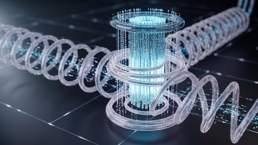
Graphene, the extraordinary single layer of carbon atoms arranged in a honeycomb pattern, has fascinated scientists and engineers worldwide due to its remarkable strength, flexibility, and conductivity. Yet, recent research has revealed there is more to graphene than meets the eye. Hidden beneath its surface, previously invisible magnetic structures are now being uncovered using a supercharged scanning tunneling microscopy (STM) technique, opening exciting new pathways for the future of electronics and quantum technologies.

In this article, we will explore the fascinating discovery of these concealed magnetic layers under graphene, explain the advanced imaging technology that made it possible, and discuss why this breakthrough could revolutionize the way we develop magnetic and electronic devices. Our goal is to present this cutting-edge science in a friendly yet authoritative way, making the complex clear for everyone from curious newcomers to seasoned professionals.
Table of Contents
Scientists Uncover Hidden Magnetic Structures Under Graphene With Supercharged Scanning Tech
| Topic | Details |
|---|---|
| Material Focus | Graphene – a one-atom-thick sheet of carbon atoms in a hexagonal lattice. |
| Discovery | Detection of hidden magnetic structures beneath graphene using enhanced STM technology. |
| Technology Used | Modified scanning tunneling microscopy capable of probing beyond the surface atomic layer. |
| Scientific Impact | Enables simultaneous atomic-scale imaging of both surface graphene and buried magnetic layers. |
| Applications | Potential advances in spintronics, quantum computing, data storage, and magnetic sensors. |
| Research Team & Source | University of Münster’s Physics Department led by Prof. Anika Schlenhoff and Dr. Maciej Bazarnik. |
The discovery of hidden magnetic structures beneath graphene using an advanced, resonant scanning tunneling microscopy technique is a significant leap forward in materials science and nanotechnology. This method provides atomic-scale visualization of magnetic and structural details that were previously inaccessible, opening the door to innovative applications in spintronics, quantum devices, and advanced electronics.
Graphene continues to be a superstar in the world of materials, and this breakthrough STM method equips researchers with an unprecedented tool to uncover its deepest secrets. With such insights, the future of ultra-small, energy-efficient, and highly functional devices looks even brighter.
For more details on the research, visit the University of Münster official research page.
Understanding Graphene and Its Magnetic Mystery

Graphene stands out as one of the most extraordinary materials discovered in recent decades. Despite being incredibly thin—just one atom thick—it possesses exceptional mechanical strength, excellent electrical and thermal conductivity, and remarkable flexibility. However, in its natural state, graphene is non-magnetic, which means it does not exhibit magnetism like familiar materials such as iron.
Yet, when graphene is combined with ultra-thin magnetic materials, such as a layer of iron underneath it, intriguing magnetic behaviors arise. Until now, scientists struggled to study these hidden magnetic interactions because the tools they had—like conventional STM—could only image the outermost atomic surface.
What Is Scanning Tunneling Microscopy (STM)?

STM is a powerful microscope invented in 1981 that allows scientists to see individual atoms and explore electronic properties at the nanoscale.
Here’s how it works in simple terms:
- A very sharp probe (think of it as an ultra-fine needle) hovers extremely close—just a few atoms away—from the surface being studied.
- A small electric voltage causes electrons to “tunnel” between the probe and the sample, a quantum mechanical effect that wouldn’t happen in everyday life.
- By scanning the probe over the surface and measuring the tunneling current, STM builds up an atomic-scale image of the surface atoms and their electronic states.
STM has been crucial in nanotechnology, but it traditionally only sees the topmost atomic layer.
Breaking New Ground: Imaging Beneath Graphene’s Surface
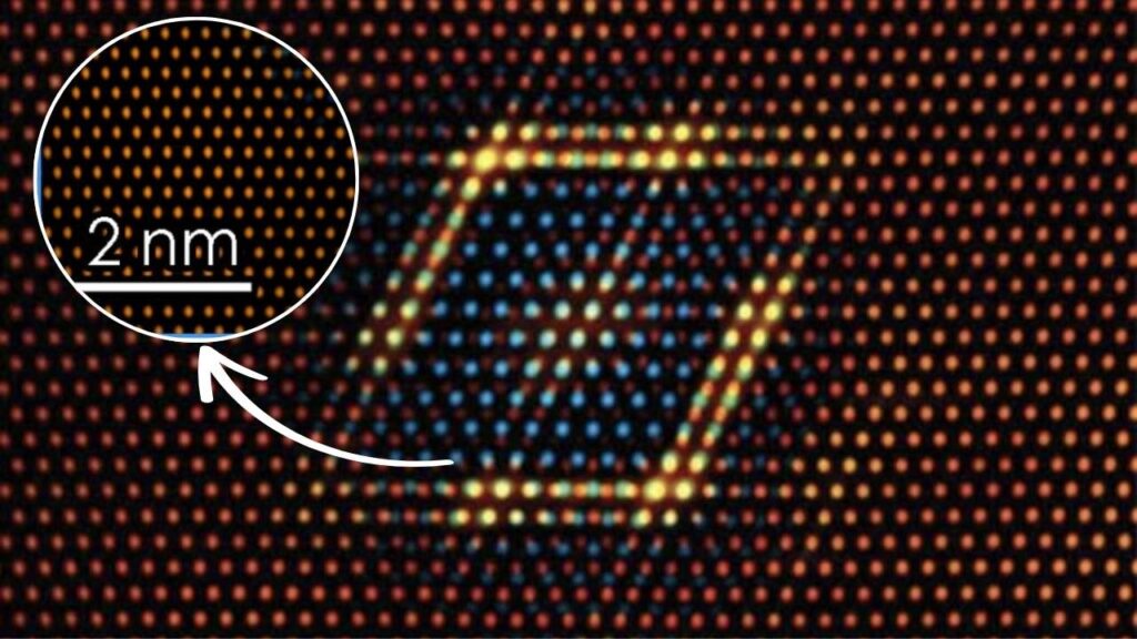
The exciting breakthrough from the University of Münster lies in a modified, resonant variant of STM. This enhanced version can probe special electronic states located above the graphene surface that extend beneath it, interacting with a buried ultra-thin iron magnetic film.

How does this work?
- The STM targets resonant electronic states near the graphene surface that physically penetrate through the graphene layer.
- These states couple magnetically with the iron atoms beneath, becoming magnetized themselves.
- This interaction allows the STM to detect and image the hidden magnetic structures under graphene, achieving atomic-scale resolution impossible before.
Additionally, this technique can resolve subtle differences in the stacking arrangement of graphene’s carbon atoms relative to the underlying iron atoms, illuminating how atomic positions influence magnetic and electronic behavior.
Why This Discovery Matters
Unveiling magnetic structures beneath graphene opens promising avenues:
- Advances Fundamental Science: Provides insight into how magnetism emerges and interacts with two-dimensional materials at the atomic level.
- Boosts Spintronics Development: Spintronics exploits the electron’s spin, a quantum property related to magnetism, to create better and more energy-efficient devices. Knowing how magnetism works under graphene could lead to new spintronic technologies.
- Enables Quantum Computing: Precise magnetic control at the nanoscale is essential for quantum devices. This imaging technique helps scientists design and optimize materials for such technologies.
- Improves Material Engineering: Understanding stacking and magnetic interactions helps in creating customized layered materials with tailored electronic and magnetic properties.
How the Discovery Was Made: A Step-By-Step Guide
Step 1: Building the Layered Material
Scientists prepare a sample consisting of an ultra-thin iron magnetic layer covered carefully with a single sheet of graphene, forming a layered system.
Step 2: Setting Up the Resonant STM
The scanning tunneling microscope is fine-tuned to focus on resonant electronic states that exist near and extend below graphene’s surface.
Step 3: Scanning and Detecting Magnetic Signals
The STM probe scans across the graphene surface, capturing detailed signals not only from graphene’s carbon lattice but also from the magnetic iron underneath.
Step 4: Imaging and Analysis
The data reveal magnetic domains hidden beneath graphene and subtle changes in how graphene atoms stack relative to iron atoms. These details offer deep insights into the magnetic and electronic coupling in layered materials.
Practical Advice for Researchers and Engineers
- Consider utilizing resonant STM techniques to explore magnetic and electronic properties in 2D layered materials.
- Focus on surface and subsurface electronic states sensitive to magnetic interactions to gain a comprehensive understanding.
- Design experiments in highly controlled environmental and temperature conditions to ensure atomic-scale resolution and stability.
- Explore combining graphene with various magnetic substrates to engineer novel devices in spintronics and quantum technology fields.
An Unexpected Physics Breakthrough Could Spark the Next Generation of Supercomputers
Why the Future of Computing Needs New Materials Beyond Moore’s Law
Graphene Breakthrough Promises Faster, Smaller, More Efficient Electronics
FAQs About Magnetic Structures Under Graphene
What makes graphene suitable for magnetic studies when it is usually non-magnetic?
While pure graphene is non-magnetic, placing it on or near magnetic materials causes electronic states in graphene to exhibit magnetic properties due to interactions across the interface.
How is this modified STM different from conventional STM?
Conventional STM detects electron tunneling from the sample’s topmost layer. The modified STM variant probes resonant states that penetrate beneath the surface, allowing imaging of buried magnetic layers.
Can this technology work with materials other than graphene?
Yes, the resonant STM method can be applied to other layered materials with hidden electronic or magnetic states, expanding its investigational scope.
Which industries stand to benefit from these findings?
Industries focused on semiconductors, quantum computing, memory storage, sensors, and spintronics will find applications for this technology.