Laser‑Patterned Color‑Center Qubits in Silicon: In the rapidly evolving field of quantum computing, precise qubit control is crucial to scaling devices from experimental setups to practical machines. Recently, Berkeley Lab researchers unveiled a groundbreaking method: using ultrashort femtosecond laser pulses to create and erase color-center qubits in silicon with atomic precision. This method enables on-demand qubit placement on silicon wafers immersed in a hydrogen-rich environment, a leap forward for quantum technology integrated with mainstream semiconductor manufacturing.

This new approach targets the creation of Ci color centers—specific atomic defects in silicon that act as qubits and emit photons in the telecom wavelength band, ideal for quantum communication networks. With such precision and compatibility, the method is poised to significantly accelerate the integration of quantum hardware with existing silicon-based technology.
Laser‑Patterned Color‑Center Qubits in Silicon
| Feature | Details |
|---|---|
| Technique | Femtosecond laser pulses in hydrogen-rich gas chamber on silicon wafers |
| Qubit Type | Ci color center: carbon interstitial + hydrogen stabilized defect |
| Photon Emission Band | Telecom S-band (~1300–1500 nm) suitable for fiber optic communication |
| Precision | Atomic-scale, on-demand creation and erasure |
| Scalability | Compatible with CMOS fabrication processes, potentially mass-producible |
| Source | Nature Communications – June 2024 (official link: nature.com) |
| Research Team | Lawrence Berkeley National Lab (ATAP & Molecular Foundry) |
Why Laser-Patterned Color-Center Qubits in Silicon Matter
Quantum bits, or qubits, are the fundamental units of quantum information. Unlike classical bits that store data as 0 or 1, qubits exploit quantum phenomena like superposition and entanglement to represent both states simultaneously, promising exponentially faster computations for specific problems.
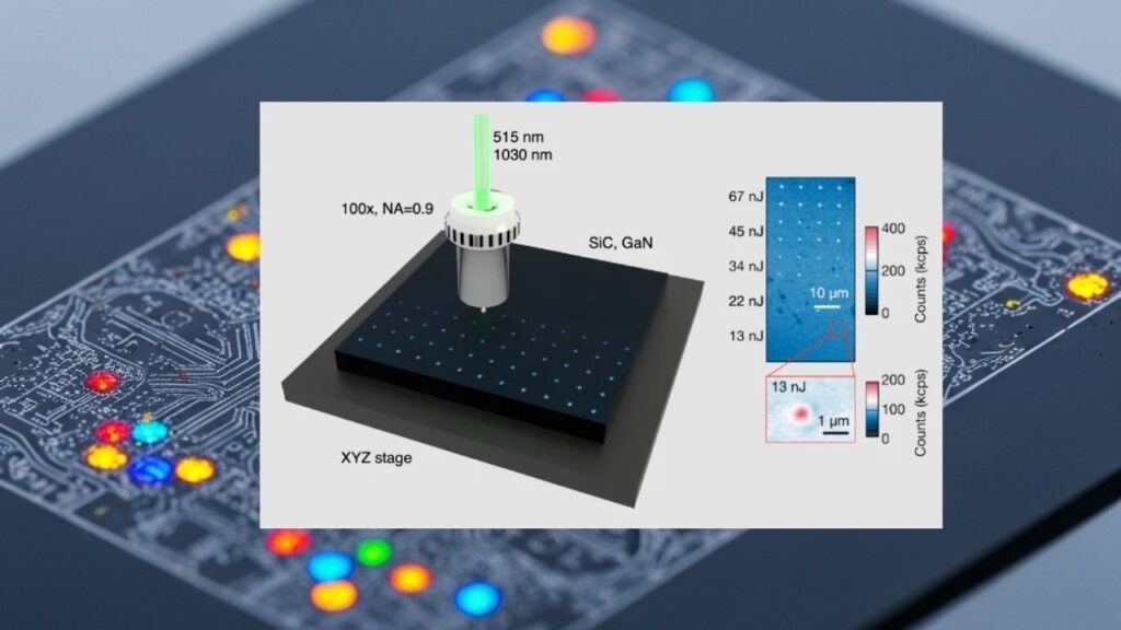
One of the main hurdles in quantum hardware development is scaling up: creating many qubits with consistent quality and arranging them precisely so they can interact as needed for computation or communication. Traditional methods like rapid thermal annealing randomly introduce qubits by heating the entire silicon wafer, resulting in unpredictable defect positions and densities.
The Berkeley Lab team’s laser-patterned technique overcomes this by:
- Writing qubits exactly where needed — using a femtosecond laser to locally generate or erase color-center defects in silicon, which serve as qubits.
- Creating qubits that emit in telecom wavelengths (~1300–1500 nm) — photons in this range travel well through optical fiber, essential for quantum networks.
- Being fully compatible with existing silicon fabrication — this opens pathways for integrating quantum devices into mass manufacturing.
This breakthrough combines quantum physics with industrial practicality, marking a significant step toward quantum computers and communication systems we can realistically build and deploy.
Berkeley Lab’s laser-patterned color-center qubit technique marks a milestone in quantum technology by marrying precise atomic defect engineering with scalable silicon fabrication. This method allows for on-demand qubit writing and erasure with atomic precision, producing qubits that emit in the telecom band—ideal for quantum communication networks.
By combining experimental photoluminescence verification, theoretical backing, and compatibility with existing semiconductor manufacturing, this work provides a clear path toward practical quantum computing and networking devices. It is a shining example of how quantum science can transition from labs to industry, moving us closer to the quantum future.
Understanding Color-Center Qubits in Silicon
At its core, a color center is a defect in a crystal lattice where an atom or group of atoms is missing or replaced, altering the material’s optical and electronic properties.
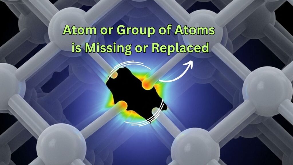
In silicon, the color centers used as qubits typically involve carbon atoms substituting or interstitially occupying positions within the silicon lattice, often stabilized by nearby hydrogen atoms.
What Makes Ci Centers Special?
The Ci center refers to a carbon atom lodged between silicon atoms in the lattice, surrounded by hydrogen. These defects possess spin states that can be manipulated and read out optically, making them promising spin-photon qubits. The photoluminescence emitted falls in the telecom wavelength range, which is significant because:
- Telecom photons travel long distances in fiber with minimal loss — crucial for building quantum communication links.
- Photon-spin coupling enables linking qubits over networks — a foundation for quantum internet and distributed quantum computing.
The presence of hydrogen is not accidental. Hydrogen stabilizes the Ci center, enhancing its brightness and spin coherence — vital for practical qubit operation.
The Laser-Patterning Process: Step-by-Step
1. Silicon Wafer and Hydrogen Environment Preparation
Silicon wafers, lightly doped with carbon, are placed inside a forming gas chamber — typically a mixture of nitrogen (N₂) and hydrogen (H₂). The hydrogen gas plays a crucial chemical role, enabling defect manipulation at the atomic level.
2. Ultrashort Femtosecond Laser Pulses
The wafer is targeted by a femtosecond laser emitting pulses lasting just a few quadrillionths of a second (10⁻¹⁵ s). This ultra-short pulse duration ensures localized energy deposition with minimal thermal diffusion, allowing precise control over defect formation.
3. Defect Creation and Erasure
- At low laser intensities, the pulses mobilize hydrogen atoms, prompting the formation of Ci color centers.
- At higher intensities, the pulses activate hydrogen to passivate or remove unwanted defects, effectively erasing previously formed qubits.
The ability to toggle between creating and removing defects at will is a game-changer, enabling complex quantum device architectures with qubits spaced and arranged precisely.
4. Photoluminescence Verification
Scientists use specialized near-infrared detectors to measure the photoluminescence spectrum of the silicon after laser processing. The presence and intensity of the telecom-band emission serve as a signature of successful Ci center formation.
Experimental and Theoretical Validation
The Berkeley Lab team backed their experimental findings with robust theoretical calculations. Using density functional theory (DFT), they demonstrated how hydrogen enhances the optical brightness of Ci centers by orders of magnitude compared to centers without hydrogen.

Experimental photoluminescence data confirmed bright emission in the telecom S-band, consistent with theoretical predictions. This two-pronged validation strengthens confidence in the laser-patterned approach as a reliable method for quantum device fabrication.
Scaling Up for Quantum Networks
A major advantage of this technique lies in its compatibility with standard silicon semiconductor processes:
- Silicon wafers used are industry-standard.
- Femtosecond laser tools can be integrated into existing chip fabrication lines.
- The method avoids global high-temperature annealing, reducing thermal budget and potential damage.
Such scalability is essential for realizing quantum processors with thousands or millions of qubits, as well as quantum communication nodes capable of linking over long distances via photons in telecom fibers.
Professional Insights from the Researchers
Kaushalya Jhuria, postdoctoral researcher at Berkeley Lab, emphasizes:
“To build scalable quantum architectures, we must precisely control qubit placement. Our laser technique offers that control, helping connect qubits reliably within quantum circuits.”
Thomas Schenkel, the principal investigator, adds:
“Our work paves a new path for industry to overcome qubit fabrication challenges by enabling precise, scalable, and CMOS-compatible qubit arrays.”
Liang Tan, computational physicist at the Molecular Foundry, notes:
“Hydrogen significantly boosts Ci center brightness, enhancing their potential for quantum communication.”
What’s Next? Future Directions and Challenges
Integration with Photonic Circuits
The next frontier is coupling these qubits with on-chip photonic waveguides and cavities to route and manipulate photons efficiently, essential for quantum logic operations and networking.
Multi-Qubit Entanglement
Creating entanglement between laser-patterned qubits on the same chip will demonstrate the capability for quantum logic gates, a crucial step toward functional quantum processors.
Exploring Other Color Centers
Researchers are also investigating T-centers and other silicon defects offering similar telecom emission but potentially better spin coherence or easier fabrication.
Industrial Adoption
Integration into CMOS fabrication lines remains a challenge but is being addressed with collaborations across national labs and semiconductor industry partners.
NASA’s SPHEREx Telescope Launches to Explore Universe’s Origins
Cleveland Clinic, IBM, and Hartree Centre Collaborate on Quantum Healthcare Research
FAQs About Laser‑Patterned Color‑Center Qubits in Silicon
Q: How does this method compare to other qubit fabrication techniques?
A: Unlike random annealing or ion implantation, laser-patterning offers on-demand precision with minimal lattice damage and is scalable using silicon CMOS technology.
Q: Why is telecom-band photon emission important?
A: Telecom wavelengths minimize loss in optical fibers, enabling practical long-distance quantum communication and network scalability.
Q: Can this technology lead to quantum computers soon?
A: While it’s a significant step, many challenges remain, including multi-qubit entanglement and error correction, but this technique addresses a critical fabrication bottleneck.
Q: What about qubit coherence times?
A: Hydrogen-stabilized Ci centers show promising spin coherence, but ongoing research seeks to optimize and extend coherence for computation.
Q: Is this approach compatible with existing chip fabrication?
A: Yes, it leverages silicon wafers and laser tools that can be integrated into standard CMOS fabs, enhancing industrial scalability.
