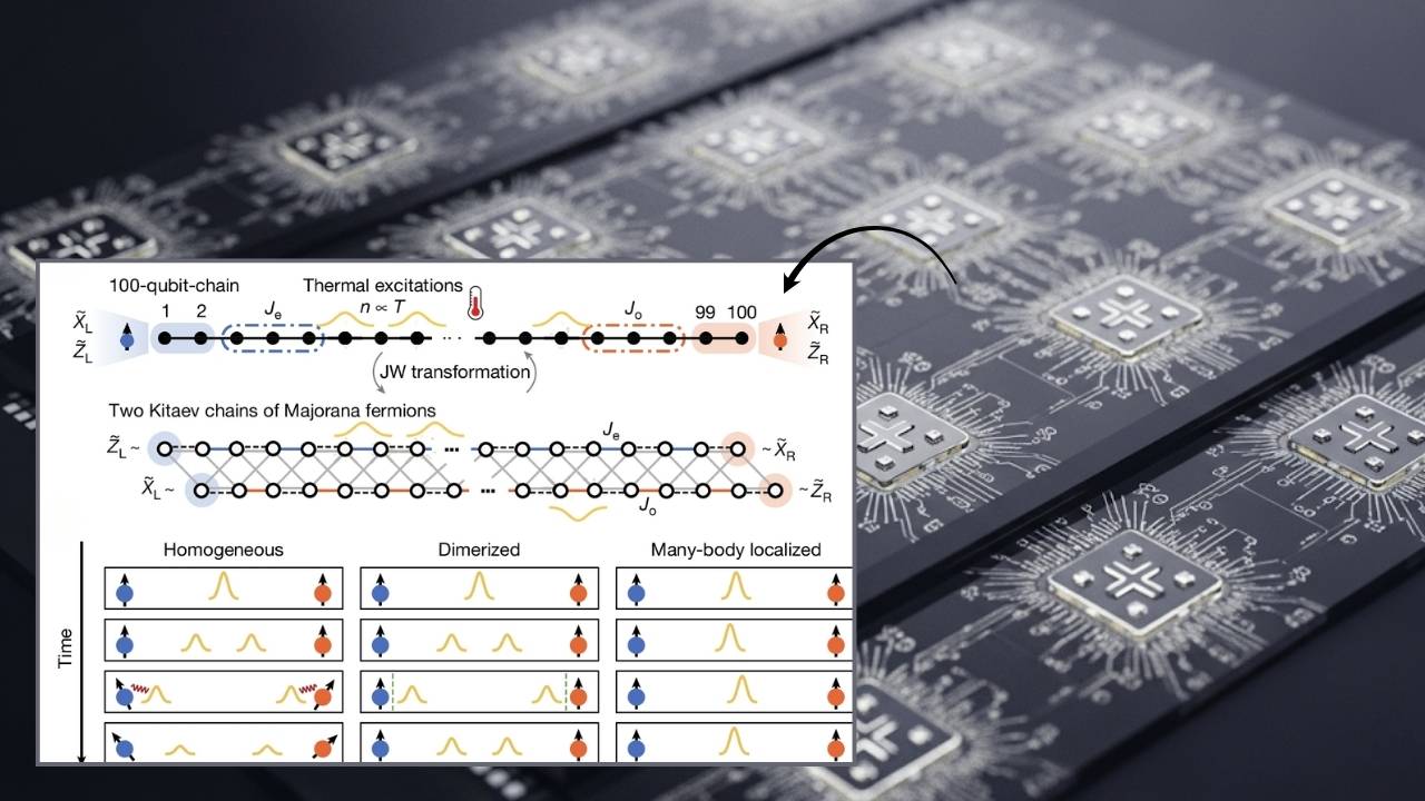
New 3D Chip Design: In a move set to transform the future of electronics, MIT introduces a new 3D chip design for improved speed and power efficiency. This breakthrough merges the strengths of gallium nitride (GaN) and silicon CMOS technology, promising faster, cooler, and more energy-efficient devices—from smartphones to data centers and even radar systems.
Let’s break down what this means, why it matters, and how it could impact both everyday users and professionals in the semiconductor industry.
New 3D Chip Design
| Feature | Details |
|---|---|
| Main Innovation | 3D integration of GaN transistors onto silicon CMOS chips using low-cost, scalable processes |
| Performance Boost | Higher signal strength, improved efficiency, reduced heat |
| Cost Efficiency | Uses tiny GaN “dielets” and copper bonding to keep manufacturing affordable |
| Compatibility | Works with existing semiconductor foundries; no need for new equipment |
| Industry Impact | Better smartphones, faster wireless, longer battery life, and enhanced radar/power electronics |
| Official Source | MIT News |
MIT’s new 3D chip design for improved speed and power efficiency is a landmark achievement in semiconductor technology. By cleverly integrating gallium nitride transistors onto silicon chips, MIT’s method delivers faster, cooler, and more energy-efficient devices—without the high costs or manufacturing headaches of previous approaches. This breakthrough is set to benefit everyone, from smartphone users to engineers building the next generation of electronics.
What Is MIT’s New 3D Chip Design?
The Basics: What Are Chips and Why Upgrade Them?
Chips, also called integrated circuits, are the “brains” inside your phone, computer, and almost every electronic device. They process information, manage power, and enable wireless communication. For decades, chips have been made mostly from silicon, a material that’s cheap, reliable, and easy to manufacture.
But as we demand more from our devices—faster speeds, better connectivity, and longer battery life—silicon alone is reaching its limits. That’s where gallium nitride (GaN) comes in.
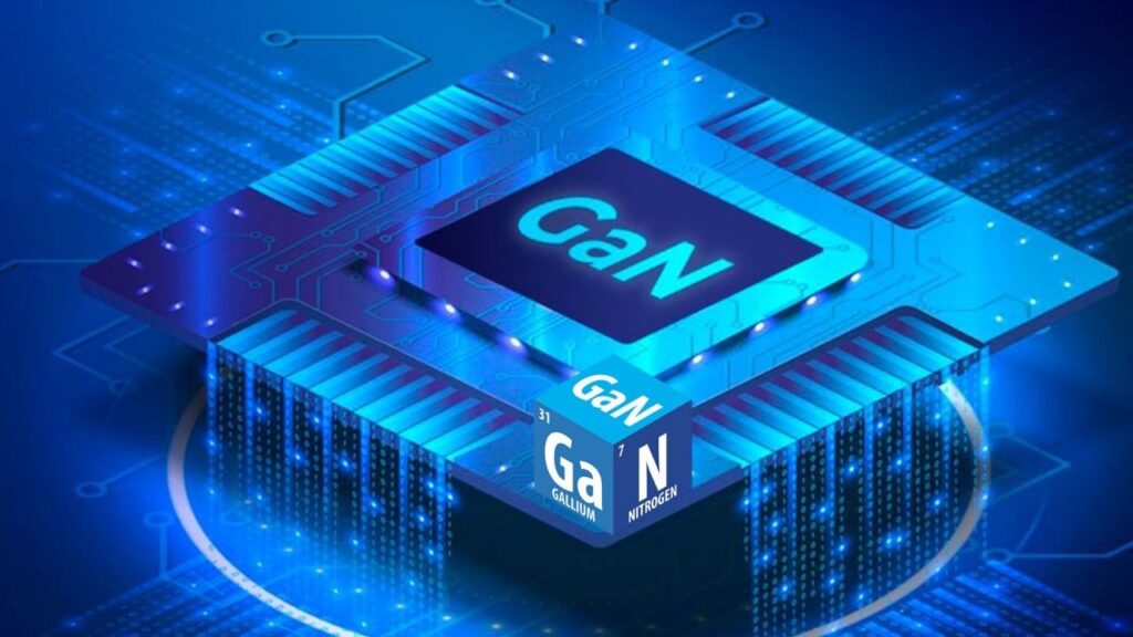
GaN is a special material that can handle much higher voltages and frequencies than silicon, making it ideal for high-speed and power-hungry applications like 5G, radar, and advanced computing.
The Breakthrough: 3D Integration of GaN and Silicon
Traditionally, combining GaN and silicon has been expensive and complex. MIT’s new method changes the game by:
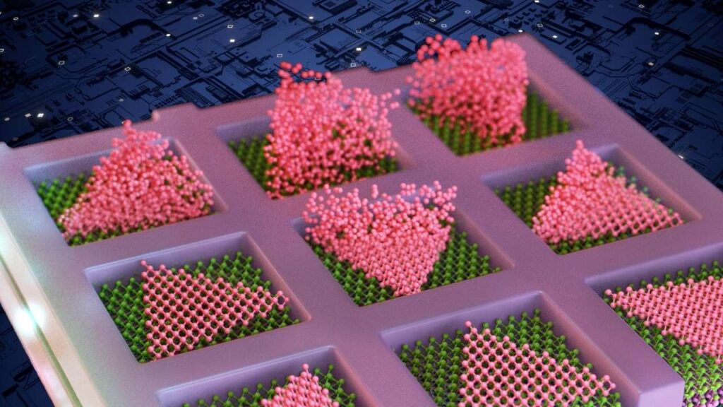
- Building tiny GaN transistors (called “dielets”) on a GaN wafer.
- Laser-cutting each dielet—each is about the size of a grain of sand (240 by 410 microns).
- Bonding the dielets onto a silicon chip using a special copper-to-copper process at low temperatures (below 400°C).
- Spreading the GaN dielets across the silicon chip to boost performance and manage heat.
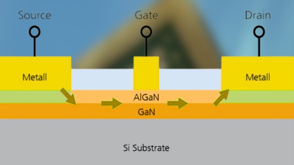
This approach is affordable, scalable, and compatible with existing chip factories, making it practical for mass production.
Why Is This Important? Real-World Impact
For Everyday Users
- Better Smartphones: Expect clearer calls, faster wireless speeds, and longer battery life. The new chips can power amplifiers that send stronger signals while using less energy.
- Cooler Devices: By distributing heat more efficiently, your phone or laptop will stay cooler, even during heavy use.
- More Reliable Electronics: Enhanced thermal management means devices will last longer and be less likely to overheat.
For Professionals and Industry
- Data Centers: Lower power consumption and improved efficiency mean big cost savings and greener operations.

- 5G and Beyond: High-speed communication systems will benefit from the faster, more robust chips.
- Radar and Defense: The cost of radar systems could drop by up to 90%, opening doors for new defense and civilian applications.
- Manufacturers: The process uses standard equipment, so companies can adopt the technology without major investments.
How Does the Technology Work? Step-by-Step Guide
1. Fabricating GaN Dielets
- GaN transistors are created on a GaN wafer.
- Each transistor is cut into a tiny dielet (240 x 410 microns).
2. Preparing the Silicon Chip
- The silicon chip (CMOS) is designed to receive the GaN dielets.
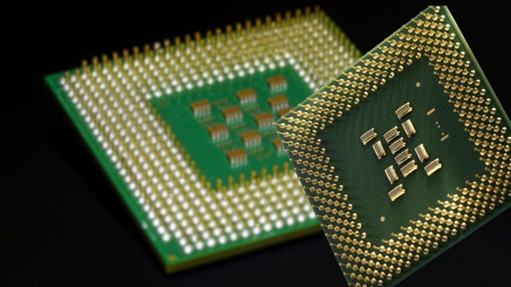
- No special modifications are needed—standard chips work fine.
3. Bonding Process
- Dielets are placed on the silicon chip using a copper-to-copper bonding method.
- The process is done at low temperatures, preserving the quality of both materials and preventing damage.
4. Integration and Testing
- The combined chip is tested for performance.
- In MIT’s demonstration, a power amplifier built this way outperformed those using only silicon, with better signal strength and efficiency.
5. Scaling Up
- The method is compatible with today’s semiconductor factories, making it ready for large-scale production.
Practical Advice: What Should Professionals and Consumers Know?
For Engineers and Designers
- Start exploring GaN-on-silicon designs for high-frequency, high-power, or thermally demanding applications.
- Leverage existing foundry partnerships—no need for new capital equipment.
- Use the integration process to minimize chip size and interconnect delays, improving overall system performance.
For Business Leaders
- Monitor developments in GaN integration—early adopters could gain a competitive edge in mobile, IoT, and defense markets.
- Prepare for new product categories enabled by smaller, more efficient, and more powerful chips.
For Consumers
- Look for next-gen devices boasting longer battery life, faster speeds, and better connectivity—these may soon be powered by MIT’s 3D chip technology.
Clear Examples: How Will This Change Devices?
- Smartphones: Power amplifiers built with the new chips will make calls clearer, data faster, and batteries last longer.
- Laptops/Tablets: Devices will run cooler, even during gaming or video editing.
- Electric Cars: Power electronics will be more efficient, helping batteries last longer and reducing charging times.
- 5G Towers: Smaller, more powerful chips will enable faster, more reliable wireless networks.
- Radar Systems: Military and weather radar can be built at a fraction of the current cost, making advanced sensing more accessible.
Physicist Resolves Long-Standing Thermodynamics Question and Refines Einstein’s Model
Cobalt-Based Catalyst Offers an Effective Alternative to Precious Metals
Researchers Identify a Previously Unknown Type of Molecular Movement
FAQs About New 3D Chip Design
What is gallium nitride (GaN), and why is it important?
GaN is a semiconductor material that can handle higher voltages and frequencies than silicon. It’s already used in LED lights, radar, and some high-end chargers. Its unique properties make it ideal for next-generation electronics.
How does this new 3D chip design differ from traditional chips?
Traditional chips are made mostly from silicon and are “flat” (2D). The new design stacks tiny GaN transistors on top of silicon chips in a 3D arrangement, boosting performance and efficiency.
Is this technology ready for mass production?
Yes. The process is compatible with existing semiconductor manufacturing equipment, making it scalable and cost-effective for broad industry use.
Will this make my phone or computer faster?
Absolutely! Devices using these new chips will be faster, use less power, and stay cooler—meaning better performance and longer battery life.
Where can I learn more about this technology?
You can find more information in the “Official Source” section of the Key Highlights table above.


