Next Generation Of Sustainable Semiconductors: In a world increasingly powered by microchips, the race to build sustainable semiconductors has taken center stage. And at the heart of this transformation? Strategic partnerships between leading universities and global tech companies. These collaborations are not only helping shape environmentally friendly manufacturing practices but also preparing a new generation of semiconductor engineers.

From Silicon Valley to Southeast Asia, academic institutions are working hand-in-hand with industry giants to advance green chip fabrication, energy efficiency, and supply chain resilience. This growing synergy between academia and industry is shaping the future of electronics—and that future looks smarter, cleaner, and more sustainable.
Table of Contents
Next Generation Of Sustainable Semiconductors
| Topic | Details |
|---|---|
| Main Focus | University-industry partnerships to develop sustainable semiconductor technologies |
| Why It Matters | Reduces environmental impact, improves supply chain stability, and creates job-ready talent |
| Top Universities Involved | MIT, Eindhoven University, Tyndall Institute, National University of Singapore, Cardiff University |
| Key Companies | Intel, ASML, Applied Materials, Hewlett Packard Enterprise |
| Investments | €180 million from ASML & Eindhoven; major NSF funding for MIT’s FUTUR-IC |
| Sustainability Goals | Reduced emissions, energy-efficient chip design, recyclable materials, and water-saving manufacturing |
| Careers Impacted | Semiconductor engineers, materials scientists, cleanroom technicians, sustainability managers |
| Global Investment Value | Over $1.2 billion in university-industry green chip collaborations since 2021 |
| Official Resource | U.S. National Science Foundation, ASML Collaboration |
What Are Sustainable Semiconductors?
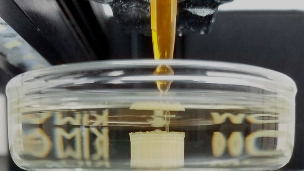
Sustainable semiconductors are designed and manufactured using eco-friendly materials, low-energy processes, and waste-reduction techniques. These practices aim to cut the environmental impact of an industry that is both energy-intensive and essential to digital infrastructure.
Why this matters:
- Semiconductor manufacturing uses more than 30 billion gallons of ultra-pure water annually.
- Chip production involves hazardous chemicals like arsenic and hydrofluoric acid.
- The electronics industry contributes significantly to global CO₂ emissions through energy consumption and logistics.
Timeline: A Decade of Collaboration
| Year | Partnership/Initiative | Impact |
|---|---|---|
| 2015 | MIT & Intel form early AI-based materials research alliance | AI-enabled green chip materials explored |
| 2018 | NUS and Applied Materials launch corporate research lab | Singapore begins developing into a global R&D hub |
| 2021 | ASML and Eindhoven announce €180M clean chip program | Establishes European talent pipeline and research facility |
| 2023 | MIT launches FUTUR-IC project with NSF and Tyndall | U.S.-Ireland collaboration to rebuild sustainable chip supply chain |
| 2024 | Cardiff expands Compound Semiconductor Manufacturing Hub | U.K. develops sovereign chip design and sustainability leadership |
The era of sustainable semiconductors has arrived—and it’s powered by unprecedented collaboration. As universities and tech companies work side by side, they’re not just solving engineering puzzles; they’re creating a blueprint for a cleaner, more resilient digital world.
For students, professionals, and innovators, this is a defining opportunity. The future of electronics isn’t just smaller or faster. It’s smarter, greener, and profoundly human.
Leading Collaborations Making Headlines
MIT and Tyndall: The FUTUR-IC Project
FUTUR-IC (FUndamental Technologies for Unconventional and Resilient Integrated Circuits) is led by MIT in partnership with Ireland’s Tyndall Institute.

- Goal: Reinvent chip manufacturing using sustainable packaging and energy-efficient fabrication.
- Approach: Advanced AI modeling, low-carbon wafer processing, and new design protocols.
- Impact: Building a resilient, low-carbon chip supply chain that meets future demands.
ASML and Eindhoven University: European Leadership
ASML, one of the world’s top semiconductor equipment makers, is investing €180 million with Eindhoven University of Technology.
- Establishing cleanroom labs, PhD tracks, and materials research programs.
- Aiming for photonics-based chip efficiency and minimal resource usage.
- Training hundreds of students and researchers over the next 10 years.
Applied Materials and NUS: Southeast Asia Innovation Hub

In Singapore, Applied Materials supports a cutting-edge research lab at NUS with a focus on:
- Advanced materials development
- Water and chemical recycling technologies
- Internships and job placements with global tech firms
Cardiff and Sheffield: The UK’s Compound Revolution
The U.K.’s Compound Semiconductor Manufacturing Hub—a joint project of Cardiff University and others—is focused on:
- Gallium nitride and silicon carbide chips that consume less power.

- Reducing chip size, heat, and emissions.
- Industry engagement with over 30 tech companies.
Global Investment Snapshot
Here’s a quick look at how much money is going into sustainable chip research globally:
| Country/Region | Estimated Investment (2021–2025) |
|---|---|
| United States | $500 million+ |
| European Union | €400 million+ |
| Singapore & Southeast Asia | $250 million+ |
| United Kingdom | £120 million+ |
| Taiwan & South Korea | $100 million+ |
Case Study: How One Student Became a Clean Tech Innovator
Emma, a materials engineering student at Eindhoven, joined ASML’s sustainable chip track in 2022.

By 2024:
- She had co-authored a paper on non-toxic etching alternatives.
- She interned at ASML’s cleanroom, contributing to real-world R&D.
- Emma is now pursuing a PhD focused on circular chip packaging.
This is just one example of how academic-industry collaboration fuels both career growth and environmental innovation.
Practical Guide to Sustainable Semiconductor Innovation
Step 1: Use Eco-Friendly Materials
- Replace rare-earth elements with earth-abundant metals.
- Explore biodegradable polymers for packaging.
Step 2: Conserve Energy
- Use AI algorithms to optimize fabrication.
- Shift to low-temperature deposition techniques.
Step 3: Save Water
- Implement recycled water systems in cleanrooms.
- Design water-efficient chemical rinse protocols.
Step 4: Reduce Emissions
- Replace gas-intensive tools with plasma etching.
- Optimize transport logistics to cut carbon output.
Step 5: Train a Green Workforce
- Introduce sustainability modules in engineering curriculums.
- Offer dual-degree programs in semiconductors and environmental science.
Future Outlook: What’s Next?
The journey toward fully sustainable chips is just beginning. Here’s what lies ahead:
- Chip-to-cloud sustainability: From hardware to data centers, sustainability will span the entire ecosystem.
- AI-powered circular design: Chips that design themselves for reuse and recycling.
- Global policy alignment: Regulations will require carbon accounting in chip supply chains.
- Green accreditation: Expect new certifications for low-impact chips akin to LEED for buildings.
Tech Meets Textiles: Smart Fabrics That Monitor Health and Power Devices
Can DNA Store the Internet? Exploring Molecular Data Storage Technologies
The Future of Displays: How MicroLEDs Are Set to Outshine OLED Technology
FAQs About Next Generation Of Sustainable Semiconductors
What Jobs Will Emerge From These Partnerships?
Roles in green fabrication, materials research, supply chain carbon audits, and ESG compliance are growing fast.
Are There Degrees Focused on Sustainable Semiconductors?
Yes. Look for programs in:
- Materials Science with Sustainability tracks
- Semiconductor Physics with Environmental Engineering modules
- Specialized master’s programs at institutions like MIT, Eindhoven, NUS
What Role Does Government Play?
Governments fund university-industry partnerships and offer tax incentives for green chip R&D and cleanroom certification standards.
Can Small Companies Join These Initiatives?
Absolutely. Many large programs offer access to startups, SMEs, and innovators through open innovation models.
How Will This Impact Consumer Electronics?
Expect future smartphones, laptops, and IoT devices to:
Use less energy
- Last longer
- Be easier to recycle