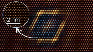
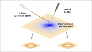
The fascinating discovery that scientists have turned pencil lead into a high-quality electron beam presents a new frontier in materials science and electron technology. Researchers at the University of Tsukuba in Japan have demonstrated that the tip of a mechanical pencil lead, when specially treated, can emit a stable and efficient electron beam, offering exciting possibilities for next-generation technological applications. This breakthrough uses a common material—graphite from pencil lead—to create a powerful electron source, potentially transforming fields such as electron microscopy and electronic devices.

In this article, we’ll explore how this discovery was made, why it matters, and how it can be practically applied, all broken down in a way everyone can understand—from curious students to professionals looking to apply this technology in their work.
Table of Contents
Scientists Turn Pencil Lead Into High-Quality Electron Beam
| Aspect | Details |
|---|---|
| Discovery Location | University of Tsukuba, Japan |
| Material Used | Mechanical pencil lead (graphite flakes) |
| Key Process | Heating fractured pencil lead tip to graphitize the surface |
| Resulting Structure | Vertically aligned graphene edges |
| Electron Emission Quality | Stable, high-quality, low electric field strength, works without ultra-high vacuum |
| Scientific Term | Field emission from graphene edges producing “dragonfly pattern” electron map |
| Potential Applications | Next-gen electron microscopes, nanotechnology, sensors, and electronic devices |
| Research Publication | Scientific Reports (DOI: 10.1038/s41598-025-11895-x) |
| Official University Link | University of Tsukuba Research News |
Turning pencil lead into a high-quality electron beam source is an extraordinary example of innovation using simple, widely available materials. The work by researchers at the University of Tsukuba leverages the unique properties of graphene inside pencil lead to produce stable and efficient electron emission. This discovery not only provides a new direction for electron beam technology but also highlights the potential for everyday materials to revolutionize advanced science and technology.
As electron-related technologies continue to grow in importance, such accessible and practical electron sources could pave the way for more affordable and efficient devices across research, industry, and healthcare.
What Is Pencil Lead Made Of?
Before diving into the science, it helps to understand what pencil lead really is. Despite the name, pencil lead contains no actual lead metal. Instead, it is mostly made of graphite, a form of carbon arranged in layers of hexagonal crystals. Graphite’s layers can slide over each other easily, which is why pencils can write smoothly on paper.
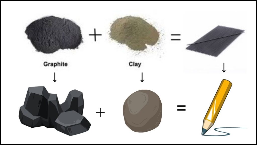
In mechanical pencil leads, the graphite is combined with clay and other materials to give the right hardness and smoothness.
Why Use Pencil Lead to Create Electron Beams?
Electron beams are streams of electrons used in tools like electron microscopes, which help scientists see objects far smaller than what light microscopes can reveal. Typically, high-quality electron sources require complex and expensive materials or devices.
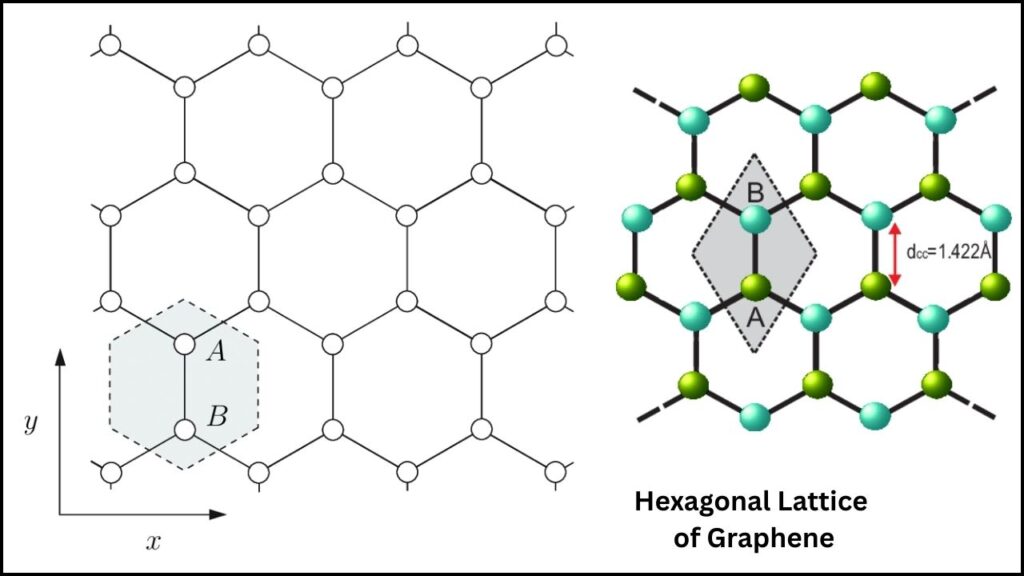
Graphene—a one-atom-thick sheet of carbon atoms arranged in a hexagonal lattice—is known for its excellent electrical properties, including the efficient emission of electrons. However, producing and arranging graphene with the right features for electron emission has been challenging and costly.
The researchers realized that mechanical pencil leads already contain graphite flakes naturally aligned along their length, which could serve as a simple and cheap source of graphene edges when treated properly.
How Did Scientists Turn Pencil Lead Into an Electron Beam?
The process involves several key steps:
1. Fracturing the Pencil Lead Tip
The researchers broke off the tip of a mechanical pencil lead, exposing a fresh surface of the graphite flakes inside.
2. Heating at High Temperature in Ultra-High Vacuum
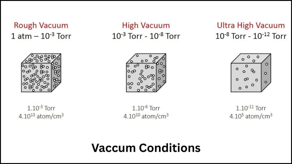
Next, the fractured surface was heated to high temperatures under ultra-high vacuum conditions. This graphitized the surface, meaning it converted it into well-ordered graphene layers.
3. Exposing Perpendicular Graphene Edges
This heating process exposed many vertically aligned graphene edges on the surface. These edges act like tiny, sharp points.
4. Electron Field Emission
When an electric field is applied, electrons are emitted from the sharp graphene edges. The emitted electrons form a distinctive “dragonfly pattern” mapping out the emission sites, confirming the graphene edges as the emission source.
5. Stable Electron Beam Under Mild Conditions
Remarkably, the electron beam emitted is stable under relatively weak electric fields and does not require strict ultra-high vacuum conditions, making it practical for various uses.
Why Is This Discovery Important?
- Accessibility: Mechanical pencil lead is cheap, easy to obtain, and readily processed. This low barrier makes graphene edge electron beam sources much more accessible than previous complex nanomaterials.
- Stability and Quality: The beam’s stability and high quality mean devices using this method could perform reliably in practical environments without expensive vacuum systems.
- New Possibilities for Technology: The research opens doors for developing affordable electron sources for electron microscopes, field emission displays, sensors, and even advanced electronics.
- Simple and Effective Method: The technique circumvents problems experienced with other graphene materials, such as difficulty controlling orientation and nanoscale arrangement.
Practical Applications of High-Quality Electron Beams
Electron beams are critical tools in many fields:
- Electron Microscopy: Provides extremely high-resolution images of biological samples, materials, and nanoparticles.
- Semiconductor Manufacturing: Used in lithography for creating microchips.
- Flat Panel Displays: Carbon nanotube and graphene electron emitters could improve display technology.
- Sensors and Nanodevices: High-quality electron beams improve sensitivity and functionality.
Using pencil lead as an electron source could significantly reduce costs and increase accessibility across these domains.
Electron Beams Now Sculpt Copper at the Nanoscale — Revolutionizing Electronics and Nanotechnology
First Electronic–Photonic Quantum Chip Built Using Commercial Foundry Technology
Researchers Discover New Method to Stabilize Ultra-Thin Materials for Next-Gen Electronics
FAQs About Scientists Turn Pencil Lead Into High-Quality Electron Beam
Q1: Is pencil lead really made of lead?
No. Pencil lead is made mainly of graphite, a form of carbon. It contains no toxic lead metal.
Q2: What is graphene and why is it important here?
Graphene is a single layer of carbon atoms arranged in a hexagonal lattice. It has exceptional electrical, thermal, and mechanical properties and can efficiently emit electrons.
Q3: Why do the graphene edges emit electrons better than other surfaces?
The edges of graphene sheets have localized electronic states that facilitate the emission of electrons when an electric field is applied.
Q4: Why is it advantageous that the electron beam works under mild conditions?
Many electron sources require ultra-high vacuum and very strong electric fields, making devices bulky and expensive. This discovery allows stable electron emission under less strict conditions, reducing cost and complexity.
Q5: What kinds of electron devices could benefit from this technology?
Electron microscopes, displays, sensors, and specialized lithography tools could all see benefits from cheaper, more stable electron sources.
How Can You Try This at Home or Work?
While the exact conditions used by the scientists—such as ultra-high vacuum heating—require professional lab equipment, the concept is simple:
- Start with a mechanical pencil lead tip.
- Carefully fracture the tip to expose fresh graphite flakes.
- Understanding the importance of graphitization and exposing graphene edges is key, which requires high-temperature treatment.
- With suitable vacuum and electrical setups, it is possible to observe electron emission patterns.
This research encourages further development of accessible methods to prepare similar materials with electron emission capabilities for broader innovation.
