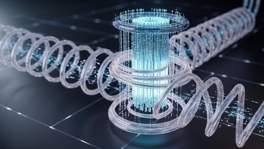
Optical vortex beams are beams of light that twist as they travel, carrying a strange and fascinating property called orbital angular momentum. These “twisted” beams have exciting applications in fields ranging from advanced microscopy and optical communication to quantum computing and optical tweezers used for manipulating tiny particles. But making these beams efficiently, in a compact, easy, and scalable way, has been a big challenge — until now.

Recent groundbreaking research has shown that van der Waals materials, a class of super-thin layered materials, can generate optical vortex beams through a phenomenon called spin-orbit coupling without needing complicated nanofabrication. This means easier, cheaper, and highly efficient vortex beam generation with the potential to transform integrated photonics and many optical technologies.
Table of Contents
Van der Waals Materials
| Feature | Details |
|---|---|
| Optical Vortex Generation Method | Spin-orbit coupling in van der Waals (vdW) materials |
| Materials Used | Hexagonal boron nitride (hBN), Molybdenum disulfide (MoS2) |
| Material Thickness Range | From sub-wavelength (320 nm) to several microns (8 µm) |
| Conversion Efficiency | Up to 0.30 for hBN (8 µm thick), 0.09 for MoS2 (320 nm thick) |
| Benefits | Fabrication-free, ultra-compact, scalable, cost-effective, high birefringence |
| Applications | Optical manipulation, quantum photonics, telecommunications, microscopy |
| Research Source | Nature Light: Sci Appl 14, 277 (2025) |
| Institutional Affiliations | Hanyang University, University of Melbourne, Peking University |
The discovery that van der Waals materials can generate optical vortex beams through spin-orbit coupling without nanofabrication marks a pivotal step forward in photonics. By leveraging their natural birefringence, these materials enable compact, efficient, and scalable optical vortex generation, poised to impact fields from quantum photonics and communications to microscopy and optical tweezing. Researchers and engineers now have a simpler, cost-effective route to harness twisted light for advanced applications.
What Are Optical Vortices and Why Do They Matter?

An optical vortex is a beam of light where the wavefront twists around the beam axis, forming a “donut”-shaped intensity pattern with a spiral phase structure. This twist carries orbital angular momentum (OAM), which can be used to encode information, sort and trap microscopic particles, or improve resolution beyond traditional optics limits.
Conventional optical vortex generation techniques include using specially designed nanostructures like fork gratings or metasurfaces. While effective, these methods require costly and time-consuming nanofabrication, limiting large-scale or dynamic applications.
Enter Van der Waals Materials: A New Horizon
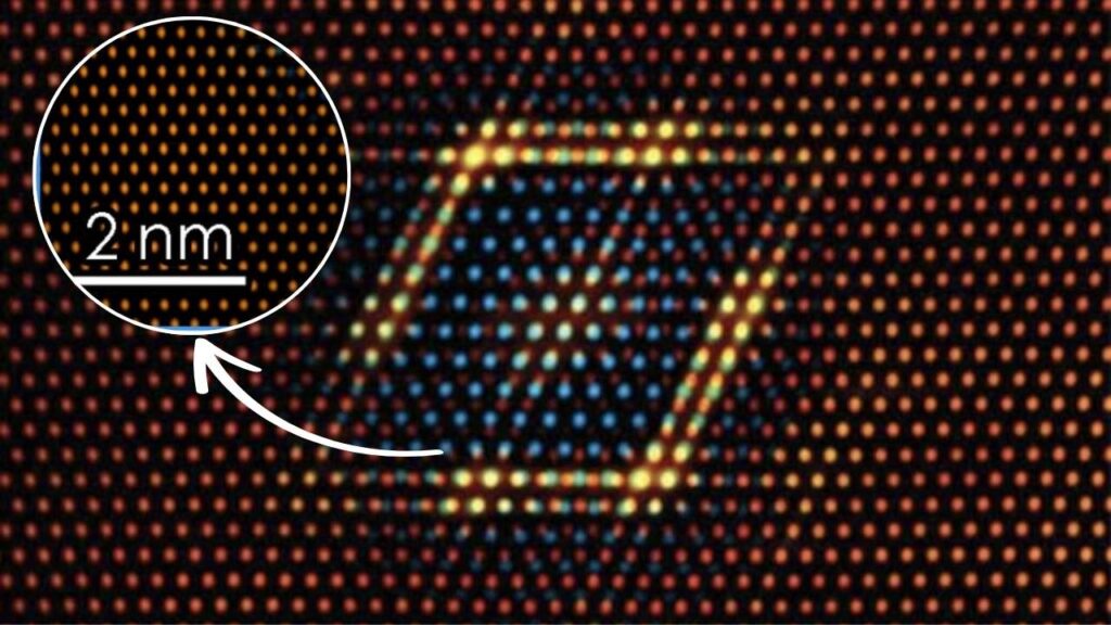
Van der Waals materials are ultra-thin layered crystals. Famous examples include graphene and hexagonal boron nitride (hBN). Their atoms are stacked and held together by weak van der Waals forces, enabling the layers to be separated down to a single atomic layer.

These materials have unique optical properties, particularly high birefringence—meaning they can split light into two beams traveling at different speeds. This property is vital for inducing spin-orbit coupling, a process by which the spin angular momentum (related to polarization) of light is converted into orbital angular momentum, generating optical vortices.
How Does Spin-Orbit Coupling in vdW Materials Create Optical Vortices?

Spin-orbit coupling (SOC) enables the transfer of light’s spin (circular polarization) into its orbital shape (vortices) without the need for external nanostructures. When circularly polarized light passes through a birefringent vdW crystal, its internal optical anisotropy causes the light’s polarization and phase to interact, producing an optical vortex.
In simple terms, the vdW crystal acts like a natural “twister” of light.
- For example, an 8-micron thick hBN crystal generates vortices with topological charges ±2, meaning the beam twists around its axis twice per wavelength.
- Even ultra-thin vdW materials like a 320-nanometer-thick MoS2 crystal show vortex generation with moderate efficiency (around 9%).

Advantages Over Traditional Methods
- Fabrication-Free: No complex lithography or etching required.
- Ultra-Compact: Can be made in sub-wavelength thicknesses.
- Scalable: Easy to integrate into photonic chips or build into large arrays.
- Efficient: Current demos show high conversion efficiency with room for optimization.
- Versatile: Potentially compatible with different light sources and wavelengths.
This breakthrough reduces manufacturing cost and complexity while allowing miniaturization critical for integrated photonics.
Practical Guide for Researchers and Engineers
Step 1: Selecting the vdW Material
- Choose materials with large intrinsic birefringence, such as hBN or MoS2.
- Consider thickness: thicker crystals generally increase conversion efficiency but may not be suitable for all applications.
Step 2: Preparing the vdW Crystals
- Mechanical exfoliation or chemical vapor deposition can yield high-quality thin flakes.
- Thickness can be measured with optical or atomic force microscopy.
Step 3: Configuring the Optical Setup
- Use circularly polarized light with precise control.
- Align the incident beam to propagate along the optical axis of the vdW crystal.
Step 4: Optimizing Spin-Orbit Coupling
- Adjust the thickness and orientation to maximize birefringence effects.
- Explore beam shapes like Bessel beams for near-unity conversion efficiency as predicted by simulations.
Step 5: Integration & Applications
- Incorporate vdW crystals into photonic integrated circuits.
- Deploy in optical communication devices, microscopy setups, or quantum photonics experiments.
Scientists Trigger a Wild Quantum Switch in Exotic Material — Superconductivity Breaks the Rules
Scientists Encode Multiple Properties Into a Single Material Using 3D Printing Magic
AI-Created 3D Materials Let You Bend Light Like Never Before
FAQs About Van der Waals Materials
Q1: What exactly is birefringence, and why is it crucial here?
Birefringence is the optical property where a material splits light into two paths with different speeds. This difference creates the phase shifts needed for spin-orbit coupling to generate vortex beams effectively.
Q2: Can vdW materials generate vortices for all light wavelengths?
While current studies focus on visible to near-infrared light, vdW materials’ layered nature allows tuning for various wavelengths pending further research.
Q3: How does this discovery impact quantum computing or communications?
Optical vortices can encode more quantum information due to their unique phase properties, making vdW materials promising for compact, efficient quantum photonic devices.
Q4: Are these materials expensive or difficult to produce?
vdW materials like hBN and MoS2 have become increasingly accessible thanks to advances in material science, making them more affordable and easier to source.